Desktop GPUs
Pre-GeForce
| Model name | Launch | Code name | Fab (nm) [2] | Transistors (million) | Die size (mm2) | Bus interface | Core clock (MHz) | Memory clock (MHz) | Core config [a] | Memory | Fillrate | Latest API support | TDP (Watts) | |||||||
|---|---|---|---|---|---|---|---|---|---|---|---|---|---|---|---|---|---|---|---|---|
| Size (MiB) | Bandwidth (GB/s) | Bus type | Bus width (bit) | MOps/s | MPixels/s | MTexels/s | MVertices/s | Direct3D | OpenGL | |||||||||||
| NV1 | May 22, 1995 | NV1 | SGS 500 nm | 1 [3] | 90 | PCI | 75 | 60 | 1:1:1 | 2 4 | 0.48 | FPM EDO VRAM | 64 | 75 | 75 | 75 | 0 | 1.0 | n/a | ? |
| Riva 128 | August 25, 1997 | NV3 | SGS 350 nm | 4 [4] | 90 | AGP 1x, [5] PCI | 100 | 100 | 4 | 1.6 | SDR | 128 | 100 | 100 | 100 | 5.0 | 1.0 | ? | ||
| Riva 128ZX | February 23, 1998 | SGS/TSMC 350 nm | AGP 2x, PCI | 8 | ? | |||||||||||||||
| Riva TNT | June 15, 1998 | NV4 | TSMC 350 nm | 7 [6] | 90 | 90 | 110 | 2:2:2 | 8 16 | 1.76 | 180 | 180 | 180 | 6.0 | 1.2 | ? | ||||
| Vanta | March 22, 1999 | NV6 | TSMC 250 nm | AGP 4x, PCI | 100 | 125 | 8 16 | 1.0 | 64 | 200 | 200 | 200 | ? | |||||||
| Vanta LT | March 2000 | AGP 2x | 80 | 100 | 8 16 | 0.8 | 160 | 160 | 160 | ? | ||||||||||
| Riva TNT2 M64 | October 1999 | AGP 4x, PCI | 125 | 150 | 8 16 32 | 1.2 | 250 | 250 | 250 | ? | ||||||||||
| Riva TNT2 | March 15, 1999 | NV5 | 15 [7] | 90 | 16 32 | 2.4 | 128 | ? | ||||||||||||
| Riva TNT2 Pro | October 12, 1999 | TSMC 220 nm | 143 | 166 | 16 32 | 2.656 | 286 | 286 | 286 | ? | ||||||||||
| Riva TNT2 Ultra | March 15, 1999 | TSMC 250 nm | 150 | 183 | 16 32 | 2.928 | 300 | 300 | 300 | ? | ||||||||||
GeForce 256 series
- All models are made via TSMC 220 nm fabrication process
- All models support Direct3D 7.0 and OpenGL 1.2
- All models support hardware Transform and Lighting (T&L) and Cube Environment Mapping
| Model name | Launch | Code name | Transistors (million) | Die size (mm2) | Bus interface | Core clock (MHz) | Memory clock (MHz) | Core config [a] | Memory | Fillrate | TDP (Watts) | ||||||
|---|---|---|---|---|---|---|---|---|---|---|---|---|---|---|---|---|---|
| Size (MiB) | Bandwidth (GB/s) | Bus type | Bus width (bit) | MOps/s | MPixels/s | MTexels/s | MVertices/s | ||||||||||
| GeForce 256 SDR [8] | Oct 11, 1999 | NV10 | 17 | 139 | AGP 4x, PCI | 120 | 166 | 4:4:4 | 32 64 | 2.656 | SDR | 128 | 480 | 480 | 480 | 0 | 13 |
| GeForce 256 DDR [9] | Dec 13, 1999 | 150 | 4.800 | DDR | 12 | ||||||||||||
GeForce2 series
- All models support Direct3D 7 and OpenGL 1.2
- All models support TwinView Dual-Display Architecture, Second-Generation Transform and Lighting (T&L),
Nvidia Shading Rasterizer (NSR), High-Definition Video Processor (HDVP) - GeForce2 MX models support Digital Vibrance Control (DVC)
| Model name | Launch | Code name | Fab (nm) [2] | Transistors (million) | Die size (mm2) | Bus interface | Core clock (MHz) | Memory clock (MHz) | Core config [a] | Memory | Fillrate | TDP (Watts) | ||||||
|---|---|---|---|---|---|---|---|---|---|---|---|---|---|---|---|---|---|---|
| Size (MiB) | Bandwidth (GB/s) | Bus type | Bus width (bit) | MOps/s | MPixels/s | MTexels/s | MVertices/s | |||||||||||
| GeForce2 MX IGP + nForce 220/420 | June 4, 2001 | NV1A (IGP)/ NV11 (MX) | TSMC 180 nm | 20 [10] | 64 | FSB | 175 | 133 | 2:4:2 | Up to 32 system RAM | 2.128 4.256 | DDR | 64 128 | 350 | 350 | 700 | 0 | 3 |
| GeForce2 MX200 | March 3, 2001 | AGP 4x, PCI | 166 | 32 64 | 1.328 | SDR | 64 | 1 | ||||||||||
| GeForce2 MX | June 28, 2000 | 2.656 | 128 | 4 | ||||||||||||||
| GeForce2 MX400 | March 3, 2001 | 200 | 166/200 (SDR) 166 (DDR) | 1.328 3.200 2.656 | SDR DDR | 64/128 (SDR) 64 (DDR) | 400 | 400 | 800 | 5 | ||||||||
| GeForce2 GTS | April 26, 2000 | NV15 | 25 [11] | 88 | AGP 4x | 166 | 4:8:4 | 5.312 | DDR | 128 | 800 | 800 | 1,600 | 6 | ||||
| GeForce2 Pro | December 5, 2000 | 200 | 6.4 | ? | ||||||||||||||
| GeForce2 Ti | October 1, 2001 | TSMC 150 nm | 250 | 1,000 | 1,000 | 2,000 | ? | |||||||||||
| GeForce2 Ultra | August 14, 2000 | TSMC 180 nm | 230 | 64 | 7.36 | ? | ||||||||||||
GeForce3 series
- All models are made via TSMC 150 nm fabrication process
- All models support Direct3D 8.0 and OpenGL 1.3
- All models support 3D Textures, Lightspeed Memory Architecture (LMA), nFiniteFX Engine, Shadow Buffers
| Model name | Launch | Code name | Transistors (million) | Die size (mm2) | Bus interface | Core clock (MHz) | Memory clock (MHz) | Core config [a] | Memory | Fillrate | TDP (Watts) | ||||||
|---|---|---|---|---|---|---|---|---|---|---|---|---|---|---|---|---|---|
| Size (MiB) | Bandwidth (GB/s) | Bus type | Bus width (bit) | MOps/s | MPixels/s | MTexels/s | MVertices/s | ||||||||||
| GeForce3 Ti200 | October 1, 2001 | NV20 | 57 | 128 | AGP 4x, PCI | 175 | 200 | 4:1:8:4 | 64 128 | 6.4 | DDR | 128 | 700 | 700 | 1400 | 43.75 | ? |
| GeForce3 | February 27, 2001 | 200 | 230 | 64 | 7.36 | 800 | 800 | 1600 | 50 | ? | |||||||
| GeForce3 Ti500 | October 1, 2001 | 240 | 250 | 64 128 | 8.0 | 960 | 960 | 1920 | 60 | 29 | |||||||
GeForce4 series
- All models are manufactured via TSMC 150 nm manufacturing process
- All models support Accuview Antialiasing (AA), Lightspeed Memory Architecture II (LMA II), nView
| Model name | Launch | Code name | Transistors (million) | Die size (mm2) | Bus interface | Core clock (MHz) | Memory clock (MHz) | Core config [a] | Memory | Fillrate | Supported API version | TDP (Watts) | |||||||
|---|---|---|---|---|---|---|---|---|---|---|---|---|---|---|---|---|---|---|---|
| Size (MiB) | Bandwidth (GB/s) | Bus type | Bus width (bit) | MOps/s | MPixels/s | MTexels/s | MVertices/s | Direct3D | OpenGL | ||||||||||
| GeForce4 MX IGP + nForce2 | October 1, 2002 | NV1F | ? | ? | FSB | 250 | 133 200 | 2:0:4:2 | Up to 128 system RAM | 2.128 6.4 | DDR | 64 128 | 500 | 500 | 1,000 | 125 | 7.0 | 1.2 | ? |
| GeForce4 MX420 | February 6, 2002 | NV17 | 29 [12] | 65 | AGP 4x PCI | 166 | 64 | 2.656 | SDR DDR | 128 (SDR) 64 (DDR) | 14 | ||||||||
| GeForce4 MX440 SE | 2002 | 133 166 | 64 128 | 2.128 5.312 [13] | DDR | 64 128 | 500 [13] 1000 | 13 | |||||||||||
| GeForce MX4000 | December 14, 2003 | NV18B | 29 | 65 | AGP 8x PCI | 166 | 2.656 | 64 | 1000 | 14 | |||||||||
| GeForce PCX4300 | February 19, 2004 | PCIe x16 | 128 | 16 | |||||||||||||||
| GeForce4 MX440 | February 6, 2002 | NV17 | 29 | 65 | AGP 4x PCI | 275 | 200 | 64 128 | 6.4 | 128 | 550 | 550 | 1,100 | 137.5 | 18 | ||||
| GeForce4 MX440 8x | September 25, 2002 | NV18 | 29 [14] | 65 | AGP 8x PCI | 166 250 | 2.656 [15] 8.0 | 64 128 | 19 | ||||||||||
| GeForce4 MX460 | February 6, 2002 | NV17 | 29 | 65 | AGP 4x PCI | 300 | 275 | 8.8 | 128 | 600 | 600 | 1,200 | 150 | 22 | |||||
| GeForce4 Ti4200 | April 16, 2002 | NV25 | 63 [16] | 142 | AGP 4x | 250 | 222 (128 MiB) 250 (64 MiB) | 4:2:8:4 | 7.104 (128 MiB) 8.0 (64 MiB) | 1,000 | 1,000 | 2,000 | 125 | 8.1 | 1.3 | 33 | |||
| GeForce4 Ti4200 8x | September 25, 2002 | NV28 | 63 [17] | 142 | AGP 8x | 250 | 8.0 | 34 | |||||||||||
| GeForce4 Ti4400 | February 6, 2002 | NV25 | 63 | 142 | AGP 4x | 275 | 275 | 128 | 8.8 | 1,100 | 1,100 | 2,200 | 137.5 | 37 | |||||
| GeForce4 Ti4400 8x (Ti4800SE [b] ) | January 20, 2003 | NV28 | 63 | 101 | AGP 8x | 38 | |||||||||||||
| GeForce4 Ti4600 | February 6, 2002 | NV25 | 63 | 142 | AGP 4x | 300 | 325 | 10.4 | 1,200 | 1,200 | 2,400 | 150 | ? | ||||||
| GeForce4 Ti4600 8x (Ti4800 [c] ) | January 20, 2003 | NV28 | 63 | 101 | AGP 8x | 43 | |||||||||||||
- ↑ Pixel shaders: vertex shaders: texture mapping units: render output units
- ↑ GeForce4 Ti4400 8x: Card manufacturers utilizing this chip labeled the card as a Ti4800SE. The surface of the chip has "Ti-8x" printed on it.
- ↑ GeForce4 Ti4600 8x: Card manufacturers utilizing this chip labeled the card as a Ti4600, and in some cases as a Ti4800. The surface of the chip has "Ti-8x" printed on it, as well as "4800" printed at the bottom.
| Model | Features | |
|---|---|---|
| nFiniteFX II Engine | Video Processing Engine (VPE) | |
| GeForce4 MX420 | No | Yes |
| GeForce4 MX440 SE | No | Yes |
| GeForce4 MX4000 | No | Yes |
| GeForce4 PCX4300 | No | Yes |
| GeForce4 MX440 | No | Yes |
| GeForce4 MX440 8X | No | Yes |
| GeForce4 MX460 | No | Yes |
| GeForce4 Ti4200 | Yes | No |
| GeForce4 Ti4200 8x | Yes | No |
| GeForce4 Ti4400 | Yes | No |
| GeForce4 Ti4400 8x | Yes | No |
| GeForce4 Ti4600 | Yes | No |
| GeForce4 Ti4600 8x | Yes | No |
GeForce FX (5xxx) series
- All models support Direct3D 9.0a and OpenGL 1.5 (2.1 (software) with latest drivers)
- The GeForce FX series runs vertex shaders in an array
| Model | Launch | Code name | Fab (nm) [2] | Transistors (million) | Die size (mm2) | Bus interface | Core clock (MHz) | Memory clock (MHz) | Core config [a] | Memory | Fillrate | TDP (Watts) | ||||||
|---|---|---|---|---|---|---|---|---|---|---|---|---|---|---|---|---|---|---|
| Size (MiB) | Bandwidth (GB/s) | Bus type | Bus width (bit) | MOperations/s | MPixels/s | MTexels/s | MVertices/s | |||||||||||
| GeForce FX 5100 | March 2003 | NV34 | TSMC 150 nm | 45 [18] | 124 | AGP 8x | 200 | 166 | 4:2:4:4 | 64 128 | 2.6 | DDR | 64 | 800 | 800 | 800 | 100.0 | ? |
| GeForce FX 5200 LE | 250 | 64 128 256 | 2.6 5.3 | 64 128 | 1,000 | 1,000 | 1,000 | 125.0 | ? | |||||||||
| GeForce FX 5200 | AGP 8x PCI | 200 | 3.2 6.4 | 64 128 | 21 | |||||||||||||
| GeForce FX 5200 Ultra | March 6, 2003 | AGP 8x | 325 | 325 | 10.4 | 128 | 1,300 | 1,300 | 1,300 | 162.5 | 32 | |||||||
| GeForce PCX 5300 | March 17, 2004 | PCIe x16 | 250 | 166 | 128 256 | 2.6 | 64 | 1,000 | 1,000 | 1,000 | 125.0 | 21 | ||||||
| GeForce FX 5500 | March 2004 | NV34B | 45 [19] | 91 | AGP 8x AGP 4x PCI | 270 | 166 200 | 64 128 256 | 2.6,3.2 5.3,6.4 | 64 128 | 1,080 | 1,080 | 1,080 | 135.0 | ? | |||
| GeForce FX 5600 XT | October 2003 | NV31 | TSMC 130 nm | 80 [20] | 121 | AGP 8x | 235 | 200 | 64 128 | 3.2 6.4 | 64 128 | 940 | 940 | 940 | 117.5 | ? | ||
| GeForce FX 5600 | March 2003 | AGP 8x PCI | 325 | 275 | 64 128 256 [21] | 8.8 | 128 | 1,300 | 1,300 | 1,300 | 162.5 | 25 | ||||||
| GeForce FX 5600 Ultra | March 6, 2003 | AGP 8x | 350 | 350 | 64 128 | 11.2 | 1,400 | 1,400 | 1,400 | 175.0 | 27 | |||||||
| GeForce FX 5600 Ultra Rev.2 | 400 | 400 | 12.8 | 1,600 | 1,600 | 1,600 | 200.0 | 31 | ||||||||||
| GeForce FX 5700 VE | September 2004 | NV36 | 82 [22] | 133 | 250 | 200 | 4:3:4:4 | 128 256 | 3.2 6.4 | 64 128 | 1000 | 1000 | 1000 | 187.5 | 20 | |||
| GeForce FX 5700 LE | March 2004 | AGP 8x PCI | 21 | |||||||||||||||
| GeForce FX 5700 | 2003 | AGP 8x | 425 | 250 | 8.0 | 128 | 1,700 | 1,700 | 1,700 | 318.7 | 20 | |||||||
| GeForce PCX 5750 | March 17, 2004 | PCIe x16 | 128 | 25 | ||||||||||||||
| GeForce FX 5700 Ultra | October 23, 2003 | AGP 8x | 475 | 453 | 128 256 | 14.4 | GDDR2 | 1,900 | 1,900 | 1,900 | 356.2 | 43 | ||||||
| GeForce FX 5700 Ultra GDDR3 | March 15, 2004 | 475 | 15.2 | GDDR3 | 38 | |||||||||||||
| GeForce FX 5800 | January 27, 2003 | NV30 | 125 [23] | 199 | 400 | 400 | 4:2:8:4 | 128 | 12.8 | GDDR2 | 1,600 | 1,600 | 3,200 | 300.0 | 55 | |||
| GeForce FX 5800 Ultra | 500 | 500 | 16.0 | 2,000 | 2,000 | 4,000 | 375.0 | 66 | ||||||||||
| GeForce FX 5900 ZT | December 15, 2003 | NV35 | 135 [24] | 207 | 325 | 350 | 4:3:8:4 | 22.4 | DDR | 256 | 1,300 | 1,300 | 2,600 | 243.7 | ? | |||
| GeForce FX 5900 XT | December 15, 2003 [25] | 390 | 1,600 | 1,600 | 3,200 | 300.0 | 48 | |||||||||||
| GeForce FX 5900 | May 2003 | 400 | 425 | 27.2 | 55 | |||||||||||||
| GeForce FX 5900 Ultra | May 12, 2003 | 450 | 128 256 | 1,800 | 1,800 | 3,600 | 337.5 | 65 | ||||||||||
| GeForce PCX 5900 | March 17, 2004 | PCIe x16 | 350 | 275 | 17.6 | 1,400 | 1,400 | 2,800 | 262.5 | 49 | ||||||||
| GeForce FX 5950 Ultra | October 23, 2003 | NV38 | 135 [26] | 207 | AGP 8x | 475 | 475 | 256 | 30.4 | 1,900 | 1,900 | 3,800 | 356.2 | 83 | ||||
| GeForce PCX 5950 | February 17, 2004 | PCIe x16 | 425 | 27.2 | GDDR3 | 83 | ||||||||||||
| Launch | Code name | Fab (nm) [2] | Transistors (million) | Die size (mm2) | Bus interface | Core clock (MHz) | Memory clock (MHz) | Core config [a] | Memory | Fillrate | TDP (Watts) | |||||||
| Size (MiB) | Bandwidth (GB/s) | Bus type | Bus width (bit) | MOperations/s | MPixels/s | MTexels/s | MVertices/s | |||||||||||
GeForce 6 (6xxx) series
- All models support Direct3D 9.0c and OpenGL 2.1
- All models support Transparency AA (starting with version 91.47 of the ForceWare drivers) and PureVideo
- [27] [28]

| Model | Launch | Code name | Fab (nm) [2] | Transistors (million) Die size (mm2) | Bus interface | Core clock (MHz) | Memory clock (MHz) | Core config [a] | Memory | Fillrate | Performance [28] (GFLOPS) [27] | TDP (Watts) | ||||||
|---|---|---|---|---|---|---|---|---|---|---|---|---|---|---|---|---|---|---|
| Size (MiB) | Bandwidth (GB/s) | Bus type | Bus width (bit) | MOperations/s | MPixels/s | MTexels/s | MVertices/s | |||||||||||
| GeForce 6100 + nForce 410 | October 20, 2005 | MCP51 | TSMC 90 nm | HyperTransport | 425 | 100–200 (DDR) 200–533 (DDR2) | 2:1:2:1 | Up to 256 system RAM | 1.6–6.4 (DDR) 3.2–17.056 (DDR2) | DDR DDR2 | 64 128 | 850 | 425 | 850 | 106.25 | 13.6 | ? | |
| GeForce 6150 SE + nForce 430 | June 2006 | MCP61 | 200 400[ citation needed ] | 3.2 16.0[ citation needed ] | DDR2 | 13.6 | ? | |||||||||||
| GeForce 6150 LE + nForce 430 | MCP61 | 100–200 (DDR) 200–533 (DDR2) | 1.6–6.4 (DDR) 3.2–17.056 (DDR2) | DDR DDR2 | 13.6 | ? | ||||||||||||
| GeForce 6150 + nForce 430 | October 20, 2005 | MCP51 | 475 | 1.6–6.4 (DDR) 3.2–17.056 (DDR2) | 950 | 475 | 950 | 118.75 | 15.2 | ? | ||||||||
| GeForce 6200 LE | April 4, 2005 | NV44 | TSMC 110 nm | 75 110 [29] | AGP 8x PCIe x16 | 350 | 266 | 128 256 | 4.256 | DDR | 64 | 700 | 700 | 700 | 87.5 | 11.2 | ? | |
| GeForce 6200A | April 4, 2005 | NV44A | 75 110 [30] | AGP 8x PCI | 300 350 [31] | 250 (DDR) 250-333 (DDR2) [31] | 4:3:4:2 | 128 256 [31] 512 [31] | 4 4-5.34 (DDR2) [32] | DDR DDR2 [33] | 64 [33] | 1,400 [31] | 700 [31] | 1400 [31] | 175 225 [33] | 21.6 25.2 | ? | |
| GeForce 6200 | October 12, 2004 (PCIe) January 17, 2005 (AGP) | NV43 | 146 154 [34] | AGP 8x PCI PCIe x16 | 300 | 275 | 4:3:4:4 | 128 256 | 8.8 | DDR | 128 | 1,200 | 1,200 | 1,200 | 225 | 21.6 | 20 | |
| GeForce 6200 TurboCache | December 15, 2004 | NV44 | 75 110 [29] | PCIe x16 | 350 | 200 275 350 | 4:3:4:2 | 128–256 System RAM incl.16/32–64/128 onboard | 3.2 4.4 5.6 | DDR | 64 | 1,400 | 700 | 1,400 | 262.5 | 25.2 | 25 | |
| GeForce 6500 | October 1, 2005 | 400 | 333 | 128 256 | 5.328 | 1,600 | 800 | 1,600 | 300 | 28.8 | ? | |||||||
| GeForce 6600 LE | 2005 | NV43 | 146 154 [34] | AGP 8x PCIe x16 | 300 | 200 | 4:3:4:4 | 6.4 | 128 | 1,200 | 1,200 | 1,200 | 225 | 21.6 | ? | |||
| GeForce 6600 | August 12, 2004 | 275 400 | 8:3:8:4 | 8.8 12.8 | DDR DDR2 | 2,400 | 2,400 | 36.0 | 26 | |||||||||
| GeForce 6600 GT | August 12, 2004 (PCIe) November 14, 2004 (AGP) | 500 | 475 (AGP) 500 (PCIe) | 15.2 (AGP) [35] 16 (PCIe) | GDDR3 | 4,000 | 2,000 | 4,000 | 375 | 60.0 | 47 | |||||||
| GeForce 6800 LE | July 22, 2004 (AGP) January 16, 2005 (PCIe) | NV40 (AGP) NV41, NV42 (PCIe) | IBM 130 nm | 222 287 (NV40) [36] 222 225 (NV41) [37] 198 222 (NV42) [38] | 320 (AGP) 325 (PCIe) | 350 | 8:4:8:8 | 128 | 22.4 | DDR | 256 | 2,560 (AGP) 2,600 (PCIe) | 2,560 (AGP) 2,600 (PCIe) | 2,560 (AGP) 2,600 (PCIe) | 320 (AGP) 325 (PCIe) | 41.0 41.6 | ? | |
| GeForce 6800 XT | September 30, 2005 | 300 (64 Bit) 325 | 266 (64 Bit) 350 500 (GDDR3) | 256 | 4.256 11.2 22.4 32 (GDDR3) | DDR DDR2 GDDR3 | 64 [39] 128 [40] 256 | 2,400 2,600 | 2,400 2,600 | 2,400 2,600 | 300 325 | 38.4<bf/>41.6 | 36 | |||||
| GeForce 6800 | April 14, 2004 (AGP) November 8, 2004 (PCIe) | 325 | 350 | 12:5:12:12 | 128 256 | 22.4 | DDR | 256 | 3,900 | 3,900 | 3,900 | 406.25 | 59.8 | 40 | ||||
| GeForce 6800 GTO | April 14, 2004 | NV45 | 222 287 (NV45) [41] | PCIe x16 | 450 | 256 | 28.8 | GDDR3 | 4,200 | 4,200 | 4,200 | 437.5 | ? | ? | ||||
| GeForce 6800 GS | December 8, 2005 (AGP) November 7, 2005 (PCIe) | NV40 (AGP) NV42 (PCIe) | TSMC 110 nm | 222 287 (NV40) [36] 198 222 (NV42) [38] | AGP 8x PCIe x16 | 350 (AGP) 425 (PCIe) | 500 | 128 256 | 32 | 5,100 | 5,100 | 5,100 | 531.25 | 64.4 78.2 | 59 | |||
| GeForce 6800 GT | May 4, 2004 (AGP) June 28, 2004 (PCIe) | NV40 (AGP) NV45 (PCIe) | IBM 130 nm | 222 287 (NV40) [36] 222 287 (NV45) [41] | AGP 8x PCIe x16 | 350 | 16:6:16:16 | 5,600 | 5,600 | 5,600 | 525 | 84.0 | 67 | |||||
| GeForce 6800 Ultra | May 4, 2004 (AGP) June 28, 2004 (PCIe) March 14, 2005 (512 MiB) | 400 | 525 (512 MiB) 550 (256 MiB) | 256 512 | 33.6 (512 MiB) 35.2 (256 MiB) | 6,400 | 6,400 | 6,400 | 600 | 96.0 | 105 | |||||||
| GeForce 6800 Ultra Extreme Edition | May 4, 2004 | NV40 | 222 287 (NV40) [36] | AGP 8x | 450 | 600 | 256 | 35.2 | 7,200 | 7,200 | 7,200 | 675 | 108.0 | ? | ||||
| Model | Launch | Code name | Fab (nm) [2] | Transistors (million) Die size (mm2) | Bus interface | Core clock (MHz) | Memory clock (MHz) | Core config [a] | Memory | Fillrate | Performance [28] (GFLOPS) [27] | TDP (Watts) | ||||||
| Size (MiB) | Bandwidth (GB/s) | Bus type | Bus width (bit) | MOperations/s | MPixels/s | MTexels/s | MVertices/s | |||||||||||
Features
| Model | Features | |||
|---|---|---|---|---|
| OpenEXR HDR | Scalable Link Interface (SLI) | TurboCache | PureVideo WMV9 Decoding | |
| GeForce 6100 | No | No | No | Limited |
| GeForce 6150 SE | No | No | Driver-Side Only | Limited |
| GeForce 6150 | No | No | No | Yes |
| GeForce 6150 LE | No | No | Driver-Side Only | Yes |
| GeForce 6200 | No | No | Yes (PCIe only) | Yes |
| GeForce 6500 | No | Yes | Yes | Yes |
| GeForce 6600 LE | Yes | Yes (No SLI Connector) | No | Yes |
| GeForce 6600 | Yes | Yes (SLI Connector or PCIe Interface) | No | Yes |
| GeForce 6600 DDR2 | Yes | Yes (SLI Connector or PCIe Interface) | No | Yes |
| GeForce 6600 GT | Yes | Yes | No | Yes |
| GeForce 6800 LE | Yes | No | No | No |
| GeForce 6800 XT | Yes | Yes (PCIe only) | No | Yes (NV42 only) |
| GeForce 6800 | Yes | Yes (PCIe only) | No | Yes (NV41, NV42 only) |
| GeForce 6800 GTO | Yes | Yes | No | No |
| GeForce 6800 GS | Yes | Yes (PCIe only) | No | Yes (NV42 only) |
| GeForce 6800 GT | Yes | Yes (PCIe only) | No | No |
| GeForce 6800 Ultra | Yes | Yes (PCIe only) | No | No |
GeForce 7 (7xxx) series
- All models support Direct3D 9.0c and OpenGL 2.1
- All models support Transparency AA (starting with version 91.47 of the ForceWare drivers)
| Model | Launch | Code name | Fab (nm) [2] | Transistors (million) | Die size (mm2) | Bus interface | Core clock (MHz) | Memory clock (MHz) | Core config [a] | Memory | Fillrate | Performance (GFLOPS) [27] [28] | TDP (Watts) | ||||||
|---|---|---|---|---|---|---|---|---|---|---|---|---|---|---|---|---|---|---|---|
| Size (MiB) | Bandwidth (GB/s) | Bus type | Bus width (bit) | MOperations/s | MPixels/s | MTexels/s | MVertices/s | ||||||||||||
| GeForce 7025 + nForce 630a | July 2007 | MCP68S | TSMC 110 nm | HyperTransport | 425 | 200 (DDR) 400 (DDR2) 933 (DDR3) | 2:1:2:2 | Up to 256 system RAM | 6.4 12.8 34 | DDR DDR2 DDR3 | 64 128 | 850 | 850 | 850 | 106.25 | 13.6 | ? | ||
| GeForce 7050PV + nForce 630a | MCP67QV | 13.6 | ? | ||||||||||||||||
| GeForce 7050 + nForce 610i/630i | MCP73 | TSMC 90 nm | HyperTransport/FSB | 500 | 333 | 5.336 | DDR2 | 64 | 1,000 | 1,000 | 1,000 | 125 | 16.0 | ? | |||||
| GeForce 7100 + nForce 630i | MCP76 | FSB | 600 | 400 | 6.4 | 1,200 | 1,200 | 1,200 | 150 | 19.2 | ? | ||||||||
| GeForce 7150 + nForce 630i | 630 | 1,260 | 1,260 | 1,260 | 157.5 | 20.2 | ? | ||||||||||||
| GeForce 7100 GS | August 8, 2006 | NV44 | TSMC 110 nm | 75 [29] | 110 | PCIe x16 | 350 | 266 333 | 4:3:4:2 | 128 256 | 2.4 4.8 | DDR2 | 32 64 | 1,400 | 700 | 1,400 | 262.5 | 25.2 | ? |
| GeForce 7200 GS | January 18, 2006 | G72 | TSMC 90 nm | 112 [42] | 81 | 450 | 400 | 2:2:4:2 | 3.2 6.4 | DDR2 | 1,800 | 900 | 1,800 | 337.5 | 18.0 | 11 | |||
| GeForce 7300 SE | March 22, 2006 | 350 | 333 | 4:3:4:2 | 128 | 2.656 5.328 | 25.2 | ? | |||||||||||
| GeForce 7300 LE | 25.2 | 13 | |||||||||||||||||
| GeForce 7300 GS | January 18, 2006 | 550 | 400 | 128 256 | 6.4 | 64 | 2,200 | 1,100 | 2,200 | 412.5 | 39.6 | 10 | |||||||
| GeForce 7300 GT | May 15, 2006 | G73 | 177 [43] | 125 | AGP 8x PCIe x16 | 350 | 325 (DDR2) 700 (GDDR3) | 8:5:8:4 | 10.4 22.4 | DDR2 GDDR3 | 128 | 2,800 | 1,400 | 2,800 | 437.5 | 47.6 | 24 | ||
| GeForce 7500 LE | 2006 | G72 | 112 [42] | 81 | PCIe x16 | 475 550 | 405 324 | 4:3:4:2 | 64 128 256 | 6.480 5.2 | DDR2 | 64 | 2,200 | 1,100 | 2,200 | 593.8 | 34.2 39.6 | 10 | |
| GeForce 7600 GS | March 22, 2006 (PCIe) July 1, 2006 (AGP) | G73 | 177 [43] | 125 | AGP 8x PCIe x16 | 400 | 400 (DDR2) 700 (GDDR3) | 12:5:12:8 | 256 | 12.8 22.4 | DDR2 GDDR3 | 128 | 4,800 | 3,200 | 4,800 | 500 | 73.6 | 30 | |
| GeForce 7600 GT | March 9, 2006 (PCIe) July 15, 2006 (AGP) | 560 | 6,720 | 4,480 | 6,720 | 700 | 103.0 | ? | |||||||||||
| GeForce 7600 GT 80 nm | January 8, 2007 | G73-B1 | TSMC 80 nm | 103.0 | 48 | ||||||||||||||
| GeForce 7650 GS | March 22, 2006 | G73 | PCIe x16 | 450 | 400 | 12.7 | DDR2 | 5,400 | 3,600 | 5,400 | 562.5 | 82.8 | ? | ||||||
| GeForce 7800 GS | February 2, 2006 | G70 | TSMC 110 nm | 302 [44] | 333 | AGP 8x | 375 | 600 | 16:8:16:8 | 38.4 | GDDR3 | 256 | 6,000 | 3,000 | 6,000 | 750 | 96.0 | 70 | |
| GeForce 7800 GT | August 11, 2005 | PCIe x16 | 400 | 500 | 20:7:20:16 | 32 | 8,000 | 6,400 | 8,000 | 700 | 118.4 | 59 | |||||||
| GeForce 7800 GTX | June 22, 2005 (256 MiB) November 14, 2005 (512 MiB) | 430 (256 MiB) 550 (512 MiB) | 600 (256 MiB) 850 (512 MiB) | 24:8:24:16 | 256 512 | 38.4 (256 MiB) 54.4 (512 MiB) | 10,320 (256 MiB) 13,200 (512 MiB) | 6,880 (256 MiB) 8800 (512 MiB) | 10,320 (256 MiB) 13,200 (512 MiB) | 860 (256 MiB) 1,100 (512 MiB) | 151.4< br/>193.6 | 100 (256 MiB) 116 (512 MiB) | |||||||
| GeForce 7900 GS | May 2006 (PCIe) April 2, 2007 (AGP) | G71 | TSMC 90 nm | 278 [45] | 196 | AGP 8x PCIe x16 | 450 | 660 | 20:7:20:16 | 256 | 42.24 | 9,000 | 7,200 | 9,000 | 787.5 | 133.2 | 50 | ||
| GeForce 7900 GT | March 9, 2006 | PCIe x16 | 24:8:24:16 | 10,800 | 10,800 | 900 | 158.4 | 65 | |||||||||||
| GeForce 7900 GTO | October 1, 2006 | 650 | 512 | 15,600 | 10,400 | 15,600 | 1,300 | 228.8 | ? | ||||||||||
| GeForce 7900 GTX | March 9, 2006 | 800 | 51.2 | 228.8 | 105 | ||||||||||||||
| GeForce 7900 GX2 | 2× G71 | 500 | 600 | 2× 24:8:24:16 | 2× 512 | 2× 38.4 | 24,000 | 16,000 | 24,000 | 2,000 | 352.0 | ? | |||||||
| GeForce 7950 GT | September 6, 2006 (PCIe) April 2, 2007 (AGP) | G71 | AGP 8x PCIe x16 | 550 | 700 | 24:8:24:16 | 512 | 44.8 | 13,200 | 8,800 | 13,200 | 1,100 | 193.6 | 90 | |||||
| GeForce 7950 GX2 | June 5, 2006 | 2× G71 | PCIe x16 | 500 | 600 | 2× 24:8:24:16 | 2× 512 | 2× 38.4 | 24,000 | 16,000 | 24,000 | 2000 | 352.0 | 136 | |||||
| Model | Launch | Code name | Fab (nm) [2] | Transistors (million) | Die size (mm2) | Bus interface | Core clock (MHz) | Memory clock (MHz) | Core config [a] | Size (MiB) | Bandwidth (GB/s) | Bus type | Bus width (bit) | MOperations/s | MPixels/s | MTexels/s | MVertices/s | Performance (GFLOPS) [27] [28] | TDP (Watts) |
| Memory | Fillrate | ||||||||||||||||||
Features
| Model | Features | ||||
|---|---|---|---|---|---|
| Gamma-correct antialiasing | 64-bit OpenEXR HDR | Scalable Link Interface (SLI) | TurboCache | Dual Link DVI | |
| GeForce 7100 GS | No | No | Yes (PCIe only, No SLI bridge) | Yes | No |
| GeForce 7200 GS | Yes | Yes | No | Yes | No |
| GeForce 7300 SE | Yes | Yes | No | Yes | No |
| GeForce 7300 LE | Yes | Yes | No | Yes | No |
| GeForce 7300 GS | Yes | Yes | Yes (PCIe only) | Yes | No |
| GeForce 7300 GT | Yes | Yes | Yes (PCIe only, No SLI bridge) | No | One port |
| GeForce 7600 GS | Yes | Yes | Yes (PCIe only) | No | One port |
| GeForce 7600 GT | Yes | Yes | Yes (PCIe only) | No | One port |
| GeForce 7600 GT (80 nm) | Yes | Yes | Yes | No | One port |
| GeForce 7650 GS (80 nm) | Yes | Yes | Yes (Depending on OEM Design) | No | One port |
| GeForce 7800 GS | Yes | Yes | No | No | One port |
| GeForce 7800 GT | Yes | Yes | Yes | No | One port |
| GeForce 7800 GTX | Yes | Yes | Yes | No | One port |
| GeForce 7800 GTX 512 | Yes | Yes | Yes | No | One port |
| GeForce 7900 GS | Yes | Yes | Yes (PCIe only) | No | Two ports |
| GeForce 7900 GT | Yes | Yes | Yes | No | Two ports |
| GeForce 7900 GTO | Yes | Yes | Yes | No | Two ports |
| GeForce 7900 GTX | Yes | Yes | Yes | No | Two ports |
| GeForce 7900 GX2 (GTX Duo) | Yes | Yes | Yes | No | Two ports |
| GeForce 7950 GT | Yes | Yes | Yes (PCIe only) | No | Two ports |
| GeForce 7950 GX2 | Yes | Yes | Yes | No | Two ports |
GeForce 8 (8xxx) series
- All models support coverage sample anti-aliasing, angle-independent anisotropic filtering, and 128-bit OpenEXR HDR.
| Model | Launch | Code name | Fab (nm) [2] | Transistors (million) | Die size (mm2) | Bus interface | Clock rate | Core config [a] | Fillrate | Memory | Processing power (GFLOPS) [b] | Supported API version | TDP (Watts) | Release Price (USD) [46] | Comments | |||||||||
|---|---|---|---|---|---|---|---|---|---|---|---|---|---|---|---|---|---|---|---|---|---|---|---|---|
| Core (MHz) | Shader (MHz) | Memory (MHz) | Pixel (GP/s) | Texture (GT/s) | Size (MiB) | Bandwidth (GB/s) | Bus type | Bus width (bit) | Single precision | Direct3D | OpenGL | OpenCL | CUDA | |||||||||||
| GeForce 8100 mGPU [47] | 2008 | MCP78 | TSMC 80 nm | Unknown | Unknown | PCIe 2.0 x16 | 500 | 1200 | 400 (system memory) | 8:8:4 | 2 | 4 | Up to 512 from system memory | 6.4 12.8 | DDR2 | 64 128 | 28.8 | 10.0 | 3.3 | n/a | n/a | Unknown | The block of decoding of HD-video PureVideo HD is disconnected | |
| GeForce 8200 mGPU [47] | Unknown | Unknown | gt | Unknown | PureVideo 3 with VP3 | |||||||||||||||||||
| GeForce 8300 mGPU [47] | Unknown | Unknown | 1500 | Up to 512 from system memory | 36 | Unknown | ||||||||||||||||||
| GeForce 8300 GS [48] | July 2007 | G86 | 210 | 127 | PCIe 1.0 x16 | 450 | 900 | 400 | 1.8 | 3.6 | 128 512 | 6.4 | 64 | 14.4 | 1.1 | 1.1 | 40 | OEM only | ||||||
| GeForce 8400 GS | June 15, 2007 | PCIe 1.0 x16 PCI | 16:8:4 | 128 256 512 | 28.8 | |||||||||||||||||||
| GeForce 8400 GS rev.2 | December 10, 2007 | G98 | TSMC 65 nm | 86 | PCIe 2.0 x16 PCIe x1 PCI | 567 | 1400 | 8:8:4 | 2.268 | 4.536 | 22.4 | 25 | ||||||||||||
| GeForce 8400 GS rev.3 | July 12, 2010 | GT218 | TSMC 40 nm | 260 | 57 | PCIe 2.0 x16 | 520 589 | 1230 | 400 (DDR2) 600 (DDR3) | 8:4:4 | 2.08 2.356 | 2.08 2.356 | 512 1024 | 4.8 6.4 9.6 | DDR2 DDR3 | 32 64 | 19.7 | 10.1 | 1.2 | |||||
| GeForce 8500 GT | April 17, 2007 | G86 | TSMC 80 nm | 210 | 127 | PCIe 1.0 x16 PCI | 450 | 900 | 400 | 16:8:4 | 1.8 | 3.6 | 256 512 1024 | 12.8 | DDR2 | 128 | 28.8 | 10.0 | 1.1 | 45 | ||||
| GeForce 8600 GS | April 2007 | G84 | 289 | 169 | PCIe 1.0 x16 | 540 | 1180 | 16:8:8 | 4.32 | 4.32 | 256 512 | 75.5 | 47 | OEM only | ||||||||||
| GeForce 8600 GT | April 17, 2007 | PCIe 1.0 x16 PCI | 1188 | 400 700 | 32:16:8 | 8.64 | 256 512 1024 | 12.8 22.4 | DDR2 GDDR3 | 76 | ||||||||||||||
| GeForce 8600 GTS | PCIe 1.0 x16 | 675 | 1450 | 1000 | 5.4 | 10.8 | 256 512 | 32 | GDDR3 | 92.8 | 71 | $140 - $199 | ||||||||||||
| GeForce 8800 GS | January 2008 | G92 | TSMC 65 nm | 754 | 324 | PCIe 2.0 x16 | 550 | 1375 | 800 | 96:48:12 | 6.6 | 26.4 | 384 768 | 38.4 | 192 | 264 | 105 | |||||||
| GeForce 8800 GTS (G80) | February 12, 2007 (320) November 8, 2006 (640) | G80 | TSMC 90 nm | 681 | 484 | PCIe 1.0 x16 | 513 | 1188 | 96:24:20 | 10.3 | 12.3 | 320 640 | 64 | 320 | 228 | 1.0 | 146 | |||||||
| GeForce 8800 GTS 112 (G80) | November 19, 2007 | 500 | 1200 | 112:28: [c] 20 | 10 | 14 | 640 | 268.8 | 150 | only XFX, EVGA and BFG models, very short-lived [51] | ||||||||||||||
| GeForce 8800 GT | October 29, 2007 (512) December 11, 2007 (256, 1024) | G92 | TSMC 65 nm | 754 | 324 | PCIe 2.0 x16 | 600 | 1500 | 700 (256) 900 (512, 1024) | 112:56:16 | 9.6 | 33.6 | 256 512 1024 | 57.6 | 256 | 336 | 1.1 | 125 | $219 - $229 (256MB) $299 - $349 (512MB) | |||||
| GeForce 8800 GTS (G92) | December 11, 2007 | 650 | 1625 | 970 | 128:64:16 | 10.4 | 41.6 | 512 | 62.1 | 416 | 135 | $349 | ||||||||||||
| GeForce 8800 GTX | November 8, 2006 | G80 | TSMC 90 nm | 681 | 484 | PCIe 1.0 x16 | 575 | 1350 | 900 | 128:32: [c] 24 | 13.8 | 18.4 | 768 | 86.4 | 384 | 345.6 | 1.0 | 145 | $500 - $600 | |||||
| GeForce 8800 Ultra | May 2, 2007 | 612 | 1500 | 1080 | 14.7 | 19.6 | 103.7 | 384 | 175 | $600 - $800 | ||||||||||||||
| Model | Launch | Code name | Fab (nm) [2] | Transistors (million) | Die size (mm2) | Bus interface | Core (MHz) | Shader (MHz) | Memory (MHz) | Core config [a] | Pixel (GP/s) | Texture (GT/s) | Size (MiB) | Bandwidth (GB/s) | Bus type | Bus width (bit) | Single precision | Direct3D | OpenGL | OpenCL | CUDA | TDP (Watts) | Comments | |
| Clock rate | Fillrate | Memory | Processing power (GFLOPS) [b] | Supported API version | ||||||||||||||||||||
- 1 2 Unified shaders: texture mapping units: render output units
- 1 2 To calculate the processing power, see Performance.
- 1 2 Full G80 contains 32 texture address units and 64 texture filtering units unlike G92 which contains 64 texture address units and 64 texture filtering units [49] [50]
Features
- Compute Capability 1.1: has support for Atomic functions, which are used to write thread-safe programs.
- Compute Capability 1.2: for details see CUDA
| Model | Features | ||||||
|---|---|---|---|---|---|---|---|
| Scalable Link Interface (SLI) | 3-Way SLI | PureVideo HD with VP1 | PureVideo 2 with VP2, BSP Engine, and AES128 Engine | PureVideo 3 with VP3, BSP Engine, and AES128 Engine | PureVideo 4 with VP4 | Compute ability | |
| GeForce 8300 GS (G86) | No | No | No | Yes | No | No | 1.1 |
| GeForce 8400 GS Rev. 2 (G98) | No | No | No | No | Yes | No | 1.1 |
| GeForce 8400 GS Rev. 3 (GT218) | No | No | No | No | No | Yes | 1.2 |
| GeForce 8500 GT | Yes | No | No | Yes | No | No | 1.1 |
| GeForce 8600 GT | Yes | No | No | Yes | No | No | 1.1 |
| GeForce 8600 GTS | Yes | No | No | Yes | No | No | 1.1 |
| GeForce 8800 GS (G92) | Yes | No | No | Yes | No | No | 1.1 |
| GeForce 8800 GTS (G80) | Yes | No | Yes | No | No | No | 1.0 |
| GeForce 8800 GTS Rev. 2 (G80) | Yes | No | Yes | No | No | No | 1.0 |
| GeForce 8800 GT (G92) | Yes | No | No | Yes | No | No | 1.1 |
| GeForce 8800 GTS (G92) | Yes | No | No | Yes | No | No | 1.1 |
| GeForce 8800 GTX | Yes | Yes | Yes | No | No | No | 1.0 |
| GeForce 8800 Ultra | Yes | Yes | Yes | No | No | No | 1.0 |
GeForce 9 (9xxx) series
- All models support Coverage Sample Anti-Aliasing, Angle-Independent Anisotropic Filtering, 128-bit OpenEXR HDR
| Model | Launch | Code name | Fab (nm) [2] | Transistors (million) | Die size (mm2) | Bus interface | Clock rate | Core config [a] | Memory | Fillrate | Processing power (GFLOPS) [b] | Supported API version | TDP (Watts) | Comments | |||||||
|---|---|---|---|---|---|---|---|---|---|---|---|---|---|---|---|---|---|---|---|---|---|
| Core (MHz) | Shader (MHz) | Memory (MHz) | Size (MiB) | Bandwidth (GB/s) | Bus type | Bus width (bit) | Pixel (GP/s) | Texture (GT/s) | Single precision | Direct3D | OpenGL | ||||||||||
| GeForce 9300 mGPU | October 2008 | MCP7A-S | 65 nm | 282 | 162 | PCIe 2.0 x16 | 450 | 1200 | 400 666 | 16:8:4 | Up to 512 from system memory | 6.4/12.8 10.664/21.328 | DDR2 DDR3 | 64 128 | 1.8 | 3.6 | 57.6 | 10.0 | 3.3 | Unknown | based on 8400 GS |
| GeForce 9400 mGPU | MCP7A-U | 580 | 1400 | 2.32 | 4.64 | 67.2 | 12 | ||||||||||||||
| GeForce 9300 GE [52] | June 2008 | G98 | TSMC 65 nm | 210 | 86 | 540 | 1300 | 500 | 8:8:4 | 256 | 6.4 [53] | DDR2 | 64 | 2.16 | 4.32 | 20.8 | 25 | ||||
| GeForce 9300 GS [52] | 567 | 1400 | 2.268 | 4.536 | 22.4 | ||||||||||||||||
| GeForce 9400 GT | August 27, 2008 | G96-200-c1 G96a G96b | TSMC 55 nm | 314 | 144 | PCIe 2.0 x16 PCI | 550 | 400 800 | 16:8:4 | 256 512 1024 | 12.8 25.6 | DDR2 GDDR3 | 128 | 2.2 | 4.4 | 44.8 | 50 | ||||
| GeForce 9500 GS | 500 | 24:12:4 | 16.0 | DDR2 | 60 | OEM | |||||||||||||||
| GeForce 9500 GT | July 29, 2008 | G96-300-C1 | UMC 65 nm | 500 800 | 32:16:8 | 16.0 25.6 | DDR2 GDDR3 | 4.4 | 8.8 | 89.6 | |||||||||||
| GeForce 9600 GS | G94a | TSMC 65 nm | 505 | 240 | PCIe 2.0 x16 | 500 | 1250 | 500 | 48:24:12 | 768 | 24.0 | DDR2 | 192 | 6 | 12 | 120 | Unknown | OEM | |||
| GeForce 9600 GSO | May 2008 | G92-150-A2 | 754 | 324 | 550 | 1375 | 800 | 96:48:12 | 384 768 1536 | 38.4 | GDDR3 | 6.6 | 26.4 | 264 | 84 | ||||||
| GeForce 9600 GSO 512 | October 2008 | G94a G94b | TSMC 65 nm TSMC 55 nm | 505 | 240 196?[ citation needed ] | 650 | 1625 | 900 | 48:24:16 | 512 | 57.6 | 256 | 10.4 | 15.6 | 156 | 90 | |||||
| GeForce 9600 GT Green Edition | 2009 | G94b | TSMC 55 nm | 196?[ citation needed ] | 600 625 | 1500 1625 | 700/900 900[ citation needed ] | 64:32:16 | 512 1024 | 44.8/57.6 57.6[ citation needed ] | 9.6 10.0 | 19.2 20.0 | 192 208 | 59 | Core Voltage = 1.00v | ||||||
| GeForce 9600 GT | February 21, 2008 | G94-300-A1 | TSMC 65 nm | 240 | 650 | 1625 | 900 | 57.6 | 10.4 | 20.8 | 208 | 95 | |||||||||
| GeForce 9800 GT Green Edition | 2009 | G92a2 G92b | TSMC/UMC 65 nm TSMC/UMC 55 nm | 754 | 324 260 | 550 | 1375 | 700 800 900 | 112:56:16 | 44.8 51.2 57.6 | 8.8 | 30.8 | 308 | 75 | Core Voltage = 1.00v | ||||||
| GeForce 9800 GT | July 2008 | G92a G92b | 65 nm UMC 55 nm | 600 | 1500 | 900 | 57.6 | 9.6 | 33.6 | 336 | 125 105 | ||||||||||
| GeForce 9800 GTX | April 1, 2008 | G92-420-A2 | TSMC 65 nm | 324 | 675 | 1688 | 1100 | 128:64:16 | 512 | 70.4 | 10.8 | 43.2 | 432 | 140 | |||||||
| GeForce 9800 GTX+ | July 16, 2008 | G92b | TSMC 55 nm | 260 | 738 | 1836 | 1100 | 512 1024 | 11.808 | 47.232 | 470 | 141 | |||||||||
| GeForce 9800 GX2 | March 18, 2008 | 2× G92 | TSMC/UMC 65 nm | 2× 754 | 2× 324 | 600 | 1500 | 1000 | 2× 128:64:16 | 2× 512 | 2× 64.0 | 2× 256 | 2× 9.6 | 2× 38.4 | 2× 384 | 197 | |||||
| Model | Launch | Code name | Fab (nm) [2] | Transistors (million) | Die size (mm2) | Bus interface | Core (MHz) | Shader (MHz) | Memory (MHz) | Core config [a] | Size (MiB) | Bandwidth (GB/s) | Bus type | Bus width (bit) | Pixel (GP/s) | Texture (GT/s) | Single precision | Direct3D | OpenGL | TDP (Watts) | Comments |
| Clock rate | Memory | Fillrate | Processing power (GFLOPS) [b] | Supported API version | |||||||||||||||||
- 1 2 Unified shaders: texture mapping units: render output units
- 1 2 To calculate the processing power see Tesla (microarchitecture)#Performance.
Features
- Compute Capability: 1.1 has support for Atomic functions, which are used to write thread-safe programs.
| Model | Features | ||
|---|---|---|---|
| Scalable Link Interface (SLI) | PureVideo 2 with VP2, BSP Engine, and AES128 Engine | PureVideo 3 with VP3, BSP Engine, and AES128 Engine | |
| GeForce 9300 GE (G98) | Yes | No | Yes |
| GeForce 9300 GS (G98) | |||
| GeForce 9400 GT | Yes | No | |
| GeForce 9500 GT | |||
| GeForce 9600 GSO | |||
| GeForce 9600 GT | |||
| GeForce 9800 GT | |||
| GeForce 9800 GTX | Yes 3-way | ||
| GeForce 9800 GTX+ | |||
| GeForce 9800 GX2 | Yes | ||
GeForce 100 series
| Model | Launch | Code name | Fab (nm) | Transistors (million) | Die size (mm2) | Bus interface | Clock rate | Core config [a] | Memory configuration | Fillrate | Processing power (GFLOPS) [b] | Supported API version | TDP (Watts) | Comments | |||||||
|---|---|---|---|---|---|---|---|---|---|---|---|---|---|---|---|---|---|---|---|---|---|
| Core (MHz) | Shader (MHz) | Memory (MHz) | Size (MiB) | Bandwidth (GB/s) | DRAM type | Bus width (bit) | Pixel (GP/s) | Texture (GT/s) | Single precision | Direct3D | OpenGL | ||||||||||
| GeForce G 100 | March 10, 2009 | G98 | TSMC 65 nm | 210 | 86 | PCIe 2.0 x16 | 567 | 1400 | 500 | 8:8:4 | 512 | 8.0 | DDR2 | 64 | 2.15 | 4.3 | 22.4 | 10.0 | 3.3 | 35 | OEM products |
| GeForce GT 120 | G96b | TSMC 55 nm | 314 | 121 | 500 | 800 | 32:16:8 | 16.0 | 128 | 4.4 | 8.8 | 89.6 | 50 | ||||||||
| GeForce GT 130 | G94b | 505 | 196 | 1250 | 500 | 48:24:12 | 1536 | 24.0 | 192 | 6 | 12 | 120 | 75 | ||||||||
| GeForce GT 140 | 650 | 1625 | 1800 | 64:32:16 | 512 1024 | 57.6 | GDDR3 | 256 | 10.4 | 20.8 | 208 | 105 | |||||||||
| GeForce GTS 150 | G92b | 754 | 260 | 738 | 1836 | 1000 | 128:64:16 | 1024 | 64.0 | 11.808 | 47.232 | 470 | 141 | ||||||||
- ↑ Unified shaders: texture mapping units: render output units
- ↑ To calculate the processing power see Tesla (microarchitecture)#Performance.
GeForce 200 series
- All models support Coverage Sample Anti-Aliasing, Angle-Independent Anisotropic Filtering, 240-bit OpenEXR HDR
| Model | Launch | Code name | Fab (nm) | Transistors (million) | Die size (mm2) | Bus interface | Clock rate | Core config [a] | Memory configuration | Fillrate | Processing power (GFLOPS) [b] | Supported API version | TDP (Watts) | Comments | Release Price (USD) | |||||||
|---|---|---|---|---|---|---|---|---|---|---|---|---|---|---|---|---|---|---|---|---|---|---|
| Core (MHz) | Shader (MHz) | Memory (GT/s) | Size (MiB) | Bandwidth (GB/s) | DRAM type | Bus width (bit) | Pixel (GP/s) | Texture (GT/s) | Single precision | Direct3D | OpenGL | |||||||||||
| GeForce 205 | November 26, 2009 | GT218 | TSMC 40 nm | 260 | 57 | PCIe 2.0 x16 | 589 | 1402 | 1 | 8:4:4 | 512 | 8 | DDR2 | 64 | 2.356 | 2.356 | 22.4 | 10.1 | 3.3 | 30.5 | OEM only | |
| GeForce 210 | October 12, 2009 | GT218-325-B1 | PCIe 2.0 x16 PCIe x1 PCI | 520 589 | 1230 1402 | 0.8 1–1.6 | 16:8:4 | 512 1024 | 4.0 8.0 12.8 | DDR2 DDR3 | 32 64 | 2.356 | 4.712 | 36.4 44.9 | 30.5 | |||||||
| GeForce GT 220 | GT216-300-A2 | TSMC 40 nm | 486 | 100 | PCIe 2.0 x16 | 615(OEM) 625 | 1335(OEM) 1360 | 1 1.58 | 48:16:8 | 512 1024 | 16.0 25.3 | DDR2 DDR3 | 64 128 | 5 | 10 | 128.2(OEM) 130.6 | 58 | |||||
| GeForce GT 230 | October 12, 2009 [54] | G94b | TSMC/UMC 55 nm | 505 | 196? | 650 | 1625 | 1.8 | 48:24:16 | 512 1024 | 57.6 | GDDR3 | 256 | 10.4 | 15.6 | 156 | 10 | 75 | OEM only | |||
| April 27, 2009 [55] | G92b | 754 | 260 | 500 | 1242 | 1 | 96:48:12 | 1536 | 24 | DDR2 | 192 | 6 | 24 | 238.5 | ||||||||
| GeForce GT 240 | November 17, 2009 | GT215-450-A2 | TSMC 40 nm | 727 | 139 | 550 | 1340 | 1.8 2 3.4(GDDR5) | 96:32:8 | 512 1024 | 28.8(OEM) 32 54.4(GDDR5) | DDR3 GDDR3 GDDR5 | 128 | 4.4 | 17.6 | 257.3 | 10.1 | 69 | ||||
| GeForce GTS 240 | July 1, 2009 [56] | G92a G92b | TSMC 65 nm TSMC/UMC 55 nm | 754 | 324 260 | 675 | 1620 | 2.2 | 112:56:16 | 1024 | 70.4 | GDDR3 | 256 | 10.8 | 37.8 | 362.9 | 10.0 | 120 | OEM only | |||
| GeForce GTS 250 | 2009 | G92b | TSMC/UMC 55 nm | 260 | 702 | 1512 | 2 | 128:64:16 | 512 1024 | 64.0 | 11.2 | 44.9 | 387 | 130 | ||||||||
| March 3, 2009 | G92-428-B1 | TSMC 65 nm TSMC/UMC 55 nm | 738 | 1836 | 2 2.2 | 512 1024 | 64.0 70.4 | 11.808 | 47.232 | 470 | 150 | Some cards are rebranded GeForce 9800 GTX+ | $150 ($130 512 MiB) | |||||||||
| GeForce GTX 260 | June 16, 2008 | GT200-100-A2 | 65 nm | 1400 | 576 | 576 | 1242 | 1.998 | 192:64:28 | 896 | 111.9 | 448 | 16.128 | 36.864 | 477 | 182 | Replaced by GTX 260 Core 216 | $400 (dropped to $270 after 3 months [57] ) | ||||
| September 16, 2008 November 27, 2008 (55 nm) | GT200-103-A2 G200-103-B2 | 65 nm 55 nm | 576 470 | 576 | 1242 1350 | 1.998 | 216:72:28 | 896 (1792) | 111.9 | 16.128 | 41.472 | 536.5 583.2 | 182 171 | 55 nm version has less TDP | $300 | |||||||
| GeForce GTX 275 | April 9, 2009 | GT200-105-B3 | TSMC/UMC 55 nm | 470 | 633 | 1404 | 2.268 | 240:80:28 | 896 (1792) | 127.0 | 17.724 | 50.6 | 674 | 219 | Effectively one-half of the GTX 295 | $250 | ||||||
| GeForce GTX 280 | June 17, 2008 | GT200-300-A2 | 65 nm | 576 | 602 | 1296 | 2.214 | 240:80:32 | 1024 | 141.7 | 512 | 19.264 | 48.16 | 622 | 236 | Replaced by GTX 285 | $650 (dropped to $430 after 3 months [57] ) | |||||
| GeForce GTX 285 | January 15, 2009 | GT200-350-B3 | TSMC/UMC 55 nm | 470 | 648 | 1476 | 2.484 | 1024 (2048) | 159.0 | 512 | 20.736 | 51.84 | 708.48 | 204 | EVGA GTX285 Classified supports 4-way SLI | $400 | ||||||
| GeForce GTX 295 | January 8, 2009 | 2× GT200-400-B3 | 2× 1400 | 2× 470 | 576 | 1242 | 1.998 | 2× 240:80:28 | 2× 896 | 2× 111.9 | 2× 448 | 2× 16.128 | 2× 46.08 | 1192.3 | 289 | Dual PCB models were replaced with a single PCB model with 2 GPUs | $500 | |||||
| Model | Launch | Code name | Fab (nm) | Transistors (million) | Die size (mm2) | Bus interface | Core (MHz) | Shader (MHz) | Memory (GT/s) | Core config [a] | Size (MiB) | Bandwidth (GB/s) | DRAM type | Bus width (bit) | Pixel (GP/s) | Texture (GT/s) | Single precision | Direct3D | OpenGL | TDP (Watts) | Comments | Release Price (USD) |
| Clock rate | Memory configuration | Fillrate | Processing power (GFLOPS) [b] | Supported API version | ||||||||||||||||||
- 1 2 Unified shaders: texture mapping units: render output units
- 1 2 To calculate the processing power see Tesla (microarchitecture)#Performance.
Features
- Compute Capability: 1.1 (G92 [GTS250] GPU)
- Compute Capability: 1.2 (GT215, GT216, GT218 GPUs)
- Compute Capability: 1.3 has double precision support for use in GPGPU applications. (GT200a/b GPUs only)
| Model | Features | ||||
|---|---|---|---|---|---|
| Scalable Link Interface (SLI) | PureVideo 2 with VP2 Engine: (BSP and 240 AES) | PureVideo 4 with VP4 Engine | |||
| GeForce 210 | No | No | Yes | ||
| GeForce GT 220 | |||||
| GeForce GT 240 | |||||
| GeForce GTS 250 | Yes 3-Way (4-way for EVGA 285 Classified) | Yes | No | ||
| GeForce GTX 260 | |||||
| GeForce GTX 260 Core 216 | |||||
| GeForce GTX 260 Core 216 (55 nm) | |||||
| GeForce GTX 275 | |||||
| GeForce GTX 280 | |||||
| GeForce GTX 285 | |||||
| GeForce GTX 295 | Yes | ||||
GeForce 300 series
| Model | Launch | Code name | Fab (nm) | Transistors (million) | Die size (mm2) | Bus interface | Clock rate | Core config [a] | Memory configuration | Fillrate | Processing power (GFLOPS) [b] | TDP (Watts) | Comments | ||||||
|---|---|---|---|---|---|---|---|---|---|---|---|---|---|---|---|---|---|---|---|
| Core (MHz) | Shader (MHz) | Memory (MHz) | Size (MiB) | Bandwidth (GB/s) | DRAM type | Bus width (bit) | Pixel (GP/s) | Texture (GT/s) | Single precision | ||||||||||
| GeForce 310 | November 27, 2009 | GT218 | TSMC 40 nm | 260 | 57 | PCIe 2.0 x16 | 589 | 1402 | 1000 | 16:8:4 | 512 | 8 | DDR2 | 64 | 2.356 | 4.712 | 44.8 | 30.5 | OEM Card, similar to Geforce 210 |
| GeForce 315 | February 2010 | GT216 | 486 | 100 | 475 | 1100 | 1580 | 48:16:4 | 512 | 12.6 | DDR3 | 3.8 | 7.6 | 105.6 | 33 | OEM Card, similar to Geforce GT220 | |||
| GeForce GT 320 | GT215 | 727 | 144 | 540 | 1302 | 72:24:8 | 1024 | 25.3 | GDDR3 | 128 | 4.32 | 12.96 | 187.5 | 43 | OEM Card | ||||
| GeForce GT 330 [58] | GT215-301-A3 [59] | 550 | 1350 | 96:32:8 | 512 | 32.00 | 128 | 4.40 | 17.60 | 257.3 | 75 | Specifications vary depending on OEM, similar to GT230 v2. | |||||||
| G92 [60] | 500 | 1250 | 256 | 51.20 | 256 | 4.000 | 24.00 | 240.0 | |||||||||||
| G92B [61] | 96:32:16 | 1024 | 16.32 | DDR2 | 128 | 8.000 | |||||||||||||
| GeForce GT 340 | GT215 | 550 | 1340 | 3400 | 96:32:8 | 512 1024 | 54.4 | GDDR5 [62] | 128 | 257.3 | 69 | OEM Card, similar to GT240 | |||||||
- ↑ Unified shaders: texture mapping units: render output units
- ↑ To calculate the processing power see Tesla (microarchitecture)#Performance.
GeForce 400 series
- All cards have a PCIe 2.0 x16 Bus interface.
- The base requirement for Vulkan 1.0 in terms of hardware features was OpenGL ES 3.1 which is a subset of OpenGL 4.3, which is supported on all Fermi and newer cards.
- Memory bandwidths stated in the following table refer to Nvidia reference designs. Actual bandwidth can be higher or lower depending on the maker of the graphic board.
| Model | Launch | Code name | Fab (nm) | Transistors (million) | Die size (mm2) | Clock rate | SM count | Core config [a] [b] | Memory configuration | Fillrate | Processing power (GFLOPS) [c] | Supported API version | TDP (Watts) [d] | Release Price (USD) | |||||||||||
|---|---|---|---|---|---|---|---|---|---|---|---|---|---|---|---|---|---|---|---|---|---|---|---|---|---|
| Core (MHz) | Shader (MHz) | Memory (MHz) | Size (GiB) | Bandwidth (GB/s) | DRAM type | Bus width (bit) | Pixel (GP/s) | Texture (GT/s) | Single precision | Double precision | Vulkan | Direct3D | OpenGL | OpenCL [e] | CUDA | ||||||||||
| GeForce 405 [f] | September 16, 2011 | GT216 GT218 | 40 nm | 486 260 | 100 57 | 475 589 | 1100 1402 | 800 790 | 1 | 48:16:8 16:8:4 | 0.5 1 | 12.6 | DDR3 | 64 | 3.8 2.36 | 7.6 4.71 | 105.6 44.86 | Unknown | n/a [66] | 10.1 | 3.3 | 1.1 | 1.2 | 30.5 | OEM |
| GeForce GT 420 | September 3, 2010 | GF108 | TSMC 40 nm | 585 | 116 | 700 | 1400 | 1800 | 48:4:4 | 0.5 | 28.8 | GDDR3 | 128 | 2.8 | 2.8 | 134.4 | Unknown | 12 FL 11_1 | 4.6 | 2.1 | 50 | ||||
| GeForce GT 430 | October 11, 2010 | GF108 GF108-300-A1 | 1600 1800 | 2 | 96:16:4 | 0.5 | 25.6 28.8 | 11.2 | 268.8 | Unknown | 1.2 | 60 | |||||||||||||
| 1800 | 0.5 1 2 | 28.8 | 128 | 268.8 | Unknown | 1.1 | 49 | $79 | |||||||||||||||||
| 1300 | 10.4 | 64 | |||||||||||||||||||||||
| GeForce GT 440 | February 1, 2011 | GF108 | 810 | 1620 | 1800 3200 | 0.5 1 | 28.8 51.2 | GDDR3 GDDR5 | 128 | 3.2 | 12.9 | 311.04 | Unknown | 65 | $100 | ||||||||||
| October 11, 2010 | GF106 | 1170 | 238 | 594 | 1189 | 1600 1800 | 3 | 144:24:24 | 1.5 3 | 43.2 | DDR3 | 192 | 4.86 | 19.44 | 342.43 | Unknown | 56 | OEM | |||||||
| GeForce GTS 450 | 790 | 1580 | 4000 | 1.5 | 96.0 | GDDR5 | 4.7 | 18.9 | 455.04 | Unknown | 106 | ||||||||||||||
| September 13, 2010 March 15, 2011 | GF106-250 GF116-200 | 783 | 1566 | 1200-1600 (GDDR3) 3608 (GDDR5) | 4 | 192:32:16 | 0.5 1 | 57.7 | 128 | 6.2 | 25.0 | 601.34 | Unknown | 106 | $129 | ||||||||||
| GeForce GTX 460 SE | November 15, 2010 | GF104-225-A1 | 1950 | 332 | 650 | 1300 | 3400 | 6 | 288:48:32 | 1 | 108.8 | 256 | 7.8 | 31.2 | 748.8 | Unknown | 150 | $160 | |||||||
| GeForce GTX 460 | October 11, 2010 | GF104 | 7 | 336:56:32 | 1 | 108.8 | 9.1 | 36.4 | 873.6 | Unknown | OEM | ||||||||||||||
| July 12, 2010 | GF104-300-KB-A1 | 675 | 1350 | 3600 | 336:56:24 | 0.75 | 86.4 | 192 | 9.4 | 37.8 | 907.2 | Unknown | $199 | ||||||||||||
| 336:56:32 | 1 2 | 115.2 | 256 | 160 | $229 | ||||||||||||||||||||
| September 24, 2011 | GF114 | 779 | 1557 | 4008 | 336:56:24 | 1 | 96.2 | 192 | 10.9 | 43.6 | 1045.6 | Unknown | $199 | ||||||||||||
| GeForce GTX 465 | May 31, 2010 | GF100-030-A3 | 3000 [67] | 529 | 608 | 1215 | 3206 | 11 | 352:44:32 | 1 | 102.7 | 256 | 13.3 | 26.7 | 855.36 | 106.92 | 1.2 | 2.0 | 200 [d] | $279 | |||||
| GeForce GTX 470 | March 26, 2010 | GF100-275-A3 | 3348 | 14 | 448:56:40 | 1.25 | 133.9 | 320 | 17.0 | 34.0 | 1088.64 | 136.08 | 215 [d] | $349 | |||||||||||
| GeForce GTX 480 | March 26, 2010 | GF100-375-A3 | 701 | 1401 | 3696 | 15 | 480:60:48 | 1.5 | 177.4 | 384 | 21.0 | 42.0 | 1344.96 | 168.12 | 250 [d] | $499 | |||||||||
| Model | Launch | Code name | Fab (nm) | Transistors (million) | Die size (mm2) | Clock rate | SM count | Core config [a] [b] | Memory configuration | Fillrate | Processing power (GFLOPS) [c] | Supported API version | TDP (Watts) [d] | Release Price (USD) | |||||||||||
| Core (MHz) | Shader (MHz) | Memory (MHz) | Size (GiB) | Bandwidth (GB/s) | DRAM type | Bus width (bit) | Pixel (GP/s) | Texture (GT/s) | Single precision | Double precision | Vulkan | Direct3D | OpenGL | OpenCL [e] | CUDA | ||||||||||
- 1 2 Unified shaders: texture mapping units: render output units
- 1 2 Each SM in the GF100 contains 4 texture filtering units for every texture address unit. The complete GF100 die contains 64 texture address units and 256 texture filtering units. [63] Each SM in the GF104/106/108 architecture contains 8 texture filtering units for every texture address unit but has doubled both addressing and filtering units. The complete GF104 die also contains 64 texture address units and 512 texture filtering units despite the halved SM count, the complete GF106 die contains 32 texture address units and 256 texture filtering units and the complete GF108 die contains 16 texture address units and 128 texture filtering units. [64]
- 1 2 To calculate the processing power see Fermi (microarchitecture)#Performance.
- 1 2 3 4 5 Note that while GTX 460's TDP is comparable to that of AMD's HD5000 series, GF100-based cards (GTX 480/470/465) are rated much lower but pull significantly more power, e.g. GTX 480 with 250W TDP consumes More power than an HD 5970 with 297W TDP. [65]
- 1 2 The 400 series is the only non-OEM family from GeForce 9 to 700 series not to include an official dual-GPU system. However, on March 18, 2011, EVGA released the first single-PCB card with dual 460s on board. The card came with 2048 MiB of memory at 3600 MHz and 672 shader processors at 1400 MHz and was offered at the MSRP of $429.
- ↑ The GeForce 405 card is a rebranded GeForce 310 which itself is a rebranded GeForce 210.
GeForce 500 series
| Model name | Launch | Code name | Fab (nm) | Transistors (million) | Die size (mm2) | Bus interface | Clock rate | SM count | Core config [a] [b] | Memory configuration | Fillrate | Processing power (GFLOPS) [c] | Supported API version | TDP (Watts) [d] | Release Price (USD) | |||||||||||
|---|---|---|---|---|---|---|---|---|---|---|---|---|---|---|---|---|---|---|---|---|---|---|---|---|---|---|
| Core (MHz) | Shader (MHz) | Memory (MHz) | Size (GiB) | Bandwidth (GB/s) | DRAM type | Bus width (bit) | Pixel (GP/s) | Texture (GT/s) | Single precision | Double precision | Vulkan | Direct3D | OpenGL | OpenCL 8 | CUDA | |||||||||||
| GeForce 510 | September 29, 2011 | GF119 | TSMC 40 nm | 292 | 79 | PCIe 2.0 x16 | 523 | 1046 | 1800 | 1 | 48:8:4 | 1 2 | 14.4 | DDR3 | 64 | 2.1 | 4.5 | 100.4 | Unknown | n/a [66] | 12 FL 11_1 | 4.6 | 1.1 | 2.1 | 25 | OEM |
| GeForce GT 520 | April 12, 2011 | PCIe 2.0 x16 PCIe 2.0 x1 PCI | 810 | 1620 | 14.4 | 3.25 | 6.5 | 155.5 | Unknown | 29 | $59 | |||||||||||||||
| GeForce GT 530 [70] | May 14, 2011 | GF108-220 | 585 | 116 | PCIe 2.0 x16 | 700 | 1400 | 2 | 96:16:4 | 28.8 | 128 | 2.8 | 11.2 | 268.8 | 22.40 | 50 | OEM | |||||||||
| GeForce GT 545 | GF116 | ~1170 | ~238 | 720 | 1440 | 3 | 144:24:16 | 1.5 3 | 43 | 192 | 11.52 | 17.28 | 415.07 | Unknown | 70 | $149 | ||||||||||
| 870 | 1740 | 3996 | 1 | 64 | GDDR5 | 128 | 13.92 | 20.88 | 501.12 | Unknown | 105 | OEM | ||||||||||||||
| GeForce GTX 550 Ti | March 15, 2011 | GF116-400 | 900 | 1800 | 4104 | 4 | 192:32:24 | 0.75+0.25 1.5 | 65.7+32.8 98.5 | 128+64 [e] 192 | 21.6 | 28.8 | 691.2 | Unknown | 116 | $149 | ||||||||||
| GeForce GTX 555 | May 14, 2011 | GF114 | 1950 | 332 | 736 | 1472 | 3828 | 6 | 288:48:24 | 1 | 91.9 | 128+64 [e] | 17.6 | 35.3 | 847.9 | Unknown | 150 | OEM | ||||||||
| GeForce GTX 560 SE | February 20, 2012 [71] | GF114-200-KB-A1 [f] | Unknown | |||||||||||||||||||||||
| GeForce GTX 560 | May 17, 2011 | GF114-325-A1 [f] | 810 | 1620 | 4008 | 7 | 336:56:32 | 1 2 | 128.1 | 256 | 25.92 | 45.36 | 1088.6 | Unknown | $199 | |||||||||||
| GeForce GTX 560 Ti | January 25, 2011 | GF114-400-A1 [f] | 822 | 1645 | 8 | 384:64:32 | 128.26 | 26.3 | 52.61 | 1263.4 | 110 | 170 | $249 | |||||||||||||
| May 30, 2011 | GF110 [g] | 3000 [73] | 520 [73] | 732 | 1464 | 3800 | 11 | 352:44:40 | 1.25 2.5 | 152 | 320 | 29.28 | 32.21 | 1030.7 | 128.83 | 210 [d] | OEM | |||||||||
| GeForce GTX 560 Ti (448 Cores) | November 29, 2011 | GF110-270-A1 [g] | 14 | 448:56:40 | 1.25 | 40.99 | 1311.7 | 163.97 | $289 | |||||||||||||||||
| GeForce GTX 570 | December 7, 2010 | GF110-275-A1 [g] | 15 | 480:60:40 | 1.25 2.5 | 43.92 | 1405.4 | 175.68 | 2.0 | 219 [d] | $349 | |||||||||||||||
| GeForce GTX 580 | November 9, 2010 | GF110-375-A1 [g] | 772 | 1544 | 4008 | 16 | 512:64:48 | 1.5 3 [h] | 192.384 | 384 | 37.05 | 49.41 | 1581.1 | 197.63 | 244 [d] [75] | $499 | ||||||||||
| GeForce GTX 590 | March 24, 2011 | 2× GF110-351-A1 | 2× 3000 | 2× 520 | 607 | 1215 | 3414 | 2× 16 | 2× 512:64:48 | 2× 1.5 | 2× 163.87 | 2× 384 | 2× 29.14 | 2× 38.85 | 2488.3 | 311.04 | 365 | $699 | ||||||||
| Model | Launch | Code name | Fab (nm) | Transistors (million) | Die size (mm2) | Bus interface | Clock rate | SM count | Core config [a] [b] | Memory configuration | Fillrate | Processing power (GFLOPS) [c] | Supported API version | TDP (Watts) [d] | Release Price (USD) | |||||||||||
| Core (MHz) | Shader (MHz) | Memory (MHz) | Size (GiB) | Bandwidth (GB/s) | DRAM type | Bus width (bit) | Pixel (GP/s) | Texture (GT/s) | Single precision | Double precision | Vulkan | Direct3D | OpenGL | OpenCL 8 | CUDA | |||||||||||
- 1 2 Unified shaders: texture mapping units: render output units
- 1 2 Each SM in the GF110 contains 4 texture filtering units for every texture address unit. The complete GF110 die contains 64 texture address units and 256 texture filtering units. [68] Each SM in the GF114/116/118 architecture contains 8 texture filtering units for every texture address unit but has doubled both addressing and filtering units.
- 1 2 To calculate the processing power see Fermi (microarchitecture)#Performance.
- 1 2 3 4 5 Similar to previous generation, GTX 580 and most likely future GTX 570[ needs update ], while reflecting its improvement over GF100, still have lower rated TDP and higher power consumption, e.g. GTX580 (243W TDP) is slightly less power hungry than GTX 480 (250W TDP). This is managed by clock throttling through drivers when a dedicated power hungry application is identified that could breach card TDP. Application name changing will disable throttling and enable full power consumption, which in some cases could be close to that of GTX480. [69]
- 1 2 1024 MiB RAM on 192-bit bus assemble with 4 x (128 MiB) + 2 x (256 MiB).
- 1 2 3 Internally referred to as GF104B [72]
- 1 2 3 4 Internally referred to as GF100B [72]
- ↑ Some companies have announced that they will be offering the GTX580 with 3GB RAM. [74]
GeForce 600 series
- Add NVENC on GTX cards
- Several 600 series cards are rebranded 400 or 500 series cards.
| Model name | Launch | Code name | Fab (nm) | Transistors (million) | Die size (mm2) | Bus interface | Clock rate | SM count | Core config [a] | Memory configuration | Fillrate | Processing power (GFLOPS) [b] | Supported API version | TDP (Watts) | Release Price (USD) | ||||||||||||
|---|---|---|---|---|---|---|---|---|---|---|---|---|---|---|---|---|---|---|---|---|---|---|---|---|---|---|---|
| Core (MHz) | Average Boost (MHz) | Max Boost (MHz) | Shader (MHz) | Memory (MHz) | Size (GiB) | Bandwidth (GB/s) | DRAM type | Bus width (bit) | Pixel (GP/s) | Texture (GT/s) | Single precision | Double precision | Vulkan [c] | Direct3D | OpenGL | OpenCL | |||||||||||
| GeForce 605 [d] | April 3, 2012 | GF119 | TSMC 40 nm | 292 | 79 | PCIe 2.0 x16 | 523 | N/a | N/a | 1046 | 898 (1796) | 1 | 48:8:4 | 0.5 1 | 14.4 | DDR3 | 64 | 2.09 | 4.2 | 100.4 | Unknown | N/a | 12 | 4.6 | 1.2 | 25 | OEM |
| GeForce GT 610 [e] | May 15, 2012 | GF119-300-A1 | PCIe 2.0 x16, PCIe x1, PCI | 810 | N/a | N/a | 1620 | 1000 1800 | 48:8:4 | 0.5 1 2 | 8 14.4 | 3.24 | 6.5 | 155.5 | Unknown | 29 | Retail | ||||||||||
| GeForce GT 620 [f] | April 3, 2012 | GF119 | PCIe 2.0 x16 | N/a | N/a | 898 (1796) | 48:8:4 | 0.5 1 | 14.4 | 6.5 | 155.5 | Unknown | 30 | OEM | |||||||||||||
| May 15, 2012 | GF108-100-KB-A1 | 585 | 116 | 700 | N/a | N/a | 1400 | 1000–1800 | 2 | 96:16:4 | 1 2 | 8–14.4 | 2.8 | 11.2 | 268.8 | Unknown | 49 | Retail | |||||||||
| GeForce GT 625 | February 19, 2013 | GF119 | 292 | 79 | 810 | N/a | N/a | 1620 | 898 (1796) | 1 | 48:8:4 | 0.5 1 | 14.4 | 3.24 | 6.5 | 155.5 | Unknown | 30 | OEM | ||||||||
| GeForce GT 630 [g] [h] | April 24, 2012 | GK107 | TSMC 28 nm | 1300 | 118 | PCIe 3.0 x16 | 875 | N/a | N/a | 875 | 891 (1782) | 192:16:16 | 1 2 | 28.5 | 128 | 14 | 14 | 336 | 14 | 1.2 | 50 | ||||||
| May 15, 2012 | GF108-400-A1 | TSMC 40 nm | 585 | 116 | PCIe 2.0 x16 | 700 | N/a | N/a | 1620 | 1600–1800 | 2 | 96:16:4 | 1 2 4 | 25.6–28.8 | 2.8 | 11.2 | 311 | Unknown | N/a | 49 | Retail | ||||||
| GF108 | 810 | N/a | N/a | 1620 | 800 (3200) | 96:16:4 | 1 | 51.2 | GDDR5 | 3.2 | 13 | 311 | Unknown | 65 | |||||||||||||
| May 29, 2013 | GK208-301-A1 | TSMC 28 nm | 1020 | 79 | PCIe 2.0 x8 | 902 | N/a | N/a | 902 | 900 (1800) | 1 | 384:16:8 | 1 2 | 14.4 | DDR3 | 64 | 7.22 | 14.44 | 692.7 | Unknown | 1.2 | 25 | |||||
| GeForce GT 635 | February 19, 2013 | GK208 | PCIe 3.0 x8 | 967 | N/a | N/a | 967 | 1001 (2002) | 384:16:8 | 16 | 7.74 | 15.5 | 742.7 | Unknown | 35 | OEM | |||||||||||
| GeForce GT 640 [i] | April 24, 2012 | GF116 | TSMC 40 nm | 1170 | 238 | PCIe 2.0 x16 | 720 | N/a | N/a | 1440 | 891 (1782) | 3 | 144:24:24 | 1.5 3 | 42.8 | 192 | 17.3 | 17.3 | 414.7 | Unknown | N/a | 75 | |||||
| GK107 | TSMC 28 nm | 1300 | 118 | PCIe 3.0 x16 | 797 | N/a | N/a | 797 | 891 (1782) | 2 | 384:32:16 | 1 2 | 28.5 | 128 | 12.8 | 25.5 | 612.1 | 25.50 | 1.2 | 50 | |||||||
| June 5, 2012 | 900 | N/a | N/a | 900 | 891 (1782) | 2 4 | 28.5 | 14.4 | 28.8 | 691.2 | 28.8 | 65 | $100 | ||||||||||||||
| April 24, 2012 | 950 | N/a | N/a | 950 | 1250 (5000) | 1 2 | 80 | GDDR5 | 15.2 | 30.4 | 729.6 | 30.40 | 75 | OEM | |||||||||||||
| May 29, 2013 | GK208-400-A1 | TSMC 28 nm | 1020 | 79 | PCIe 2.0 x8 | 1046 | N/a | N/a | 1046 | 1252 (5008) | 384:16:8 | 1 | 40.1 | 64 | 8.37 | 16.7 | 803.3 | Unknown | 49 | ||||||||
| GeForce GT 645 [j] | April 24, 2012 | GF114-400-A1 | TSMC 40 nm | 1950 | 332 | PCIe 2.0 x16 | 776 | N/a | N/a | 1552 | 1914 | 6 | 288:48:24 | 91.9 | 192 | 18.6 | 37.3 | 894 | Unknown | N/a | 140 | OEM | |||||
| GeForce GTX 645 | April 22, 2013 | GK106 | TSMC 28 nm | 2540 | 221 | PCIe 3.0 x16 | 823.5 | 888.5 | N/a | 823 | 1000 (4000) | 3 | 576:48:16 | 64 | 128 | 14.16 | 39.5 | 948.1 | 39.53 | 1.2 | 64 | ||||||
| GeForce GTX 650 | September 13, 2012 | GK107-450-A2 | 1300 | 118 | 1058 | N/a | N/a | 1058 | 1250 (5000) | 2 | 384:32:16 | 1 2 | 80 | 16.9 | 33.8 | 812.54 | 33.86 | $110 | |||||||||
| November 27, 2013 [76] | GK-106-400-A1 | 2540 | 221 | N/a | 65 | ? | |||||||||||||||||||||
| GeForce GTX 650 Ti | October 9, 2012 | GK106-220-A1 | 928 | N/a | N/a | 928 | 1350 (5400) | 4 | 768:64:16 | 86.4 | 14.8 | 59.4 | 1425.41 | 59.39 | 110 | $150 (130) | |||||||||||
| GeForce GTX 650 Ti (Boost) | March 26, 2013 | GK106-240-A1 | 980 | 1032 | N/a | 980 | 1502 (6008) | 768:64:24 | 144.2 | 192 | 23.5 | 62.7 | 1505.28 | 62.72 | 134 | $170 (150) | |||||||||||
| GeForce GTX 660 | September 13, 2012 | GK106-400-A1 | 1084 | 1502 (6008) | 5 | 960:80:24 | 1.5+0.5 3 | 96.1+48.1 144.2 | 128+64 192 | 23.5 | 78.4 | 1881.6 | 78.40 | 140 | $230 (180) | ||||||||||||
| August 22, 2012 | GK104-200-KD-A2 | 3540 | 294 | 823.5 | 888.5 | 899 | 823 | 1450 (5800) | 6 | 1152:96:24 1152:96:32 | 1.5 2 3 | 139 186 | 192 256 | 19.8 | 79 | 2108.6 | 79.06 | 130 | OEM | ||||||||
| GeForce GTX 660 Ti | August 16, 2012 | GK104-300-KD-A2 | 915 | 980 | 1058 | 915 | 1502 (6008) | 7 | 1344:112:24 | 2 | 96.1+48.1 144.2 | 128+64 192 | 22.0 | 102.5 | 2459.52 | 102.48 | 150 | $300 | |||||||||
| GeForce GTX 670 | May 10, 2012 | GK104-325-A2 | 1084 | 1502 (6008) | 1344:112:32 | 2 4 | 192.256 | 256 | 29.3 | 102.5 | 2459.52 | 102.48 | 170 | $400 | |||||||||||||
| GeForce GTX 680 | March 22, 2012 | GK104-400-A2 | 1006 [77] | 1058 | 1110 | 1006 | 1502 (6008) | 8 | 1536:128:32 | 192.256 | 32.2 | 128.8 | 3090.43 | 128.77 | 195 | $500 | |||||||||||
| GeForce GTX 690 | April 29, 2012 | 2× GK104-355-A2 | 2× 3540 | 2× 294 | 915 | 1019 | 1058 | 915 | 1502 (6008) | 2× 8 | 2× 1536:128:32 | 2× 2 | 2× 192.256 | 2× 256 | 2× 29.28 | 2× 117.12 | 2× 2810.88 | 2× 117.12 | 300 | $1000 | |||||||
| Model | Launch | Code name | Fab (nm) | Transistors (million) | Die size (mm2) | Bus interface | Clock rate | SM count | Core config [a] | Memory configuration | Fillrate | Processing power (GFLOPS) [b] | Supported API version | TDP (Watts) | Release Price (USD) | ||||||||||||
| Core (MHz) | Average Boost (MHz) | Max Boost (MHz) | Shader (MHz) | Memory (MHz) | Size (GiB) | Bandwidth (GB/s) | DRAM type | Bus width (bit) | Pixel (GP/s) | Texture (GT/s) | Single precision | Double precision | Vulkan [c] | Direct3D | OpenGL | OpenCL | |||||||||||
- 1 2 Unified shaders: texture mapping units: render output units
- 1 2 To calculate the processing power see Kepler (microarchitecture)#Performance, or Fermi (microarchitecture)#Performance.
- 1 2 Vulkan 1.2 is only supported on Kepler cards. [66]
- ↑ The GeForce 605 (OEM) card is a rebranded GeForce 510.
- ↑ The GeForce GT 610 card is a rebranded GeForce GT 520.
- ↑ The GeForce GT 620 (OEM) card is a rebranded GeForce GT 520.
- ↑ The GeForce GT 630 (DDR3, 128-bit, retail) card is a rebranded GeForce GT 430 (DDR3, 128-bit).
- ↑ The GeForce GT 630 (GDDR5) card is a rebranded GeForce GT 440 (GDDR5).
- ↑ The GeForce GT 640 (OEM) GF116 card is a rebranded GeForce GT 545 (DDR3).
- ↑ The GeForce GT 645 (OEM) card is a rebranded GeForce GTX 560 SE.
GeForce 700 series
The GeForce 700 series for desktop. The GM107-chips are Maxwell-based, the GF1xx are Fermi-based, and the GKxxx-chips Kepler.
- Improve NVENC
| Model name | Launch | Code name | Fab (nm) | Transistors (million) | Die size (mm2) | Bus interface | Clock rate | SMX count | Core config [a] | Memory configuration | Fillrate | Processing power (GFLOPS) [b] | Supported API version | TDP (Watts) | Release Price (USD) | |||||||||||
|---|---|---|---|---|---|---|---|---|---|---|---|---|---|---|---|---|---|---|---|---|---|---|---|---|---|---|
| Base (MHz) | Average Boost (MHz) | Max Boost [c] (MHz) | Memory (MHz) | Size (GiB) | Bandwidth (GB/s) | DRAM type | Bus width (bit) | Pixel (GP/s) | Texture (GT/s) | Single precision | Double precision | Vulkan [d] | Direct3D [e] | OpenGL | OpenCL | |||||||||||
| GeForce GT 705 [80] [f] | March 27, 2014 | GF119-300-A1 | TSMC 40 nm | 292 | 79 | PCIe 2.0 x16 | 810 | N/a | N/a | 898 (1796) | 1 | 48:8:4 | 0.5 1 | 14.4 | DDR3 | 64 | 3.24 | 6.5 | 155.5 | 19.4 | n/a | 12 | 4.6 | 1.1 | 29 | OEM |
| GeForce GT 710 [81] | GK208-301-A1 | TSMC 28 nm | 1020 | 79 | PCIe 2.0 x8 | 823 | N/a | N/a | 900 (1800) | 192:16:8 | 0.5 | 64 | 6.6 | 13.2 | 316.0 | 13.2 | 1.2 | 1.2 | ||||||||
| January 26, 2016 | GK208-203-B1 | PCIe 2.0 x8, PCIe x1 | 954 | N/a | N/a | 900 (1800) 1253 (5010) | 192:16:8 | 1 2 | 14.4 40.0 | DDR3 GDDR5 | 7.6 | 15.3 | 366 | 15.3 | 19 | $35–45 | ||||||||||
| GeForce GT 720 [82] | March 27, 2014 | GK208-201-B1 | PCIe 2.0 x8 | 797 | N/a | N/a | 900 (1800) 1253 (5010) | 192:16:8 | 1 2 | 14.4 40.0 | 6.4 | 12.8 | 306 | 12.8 | $49–59 | |||||||||||
| GeForce GT 730 [83] [g] [h] | June 18, 2014 | GK208-301-A1 | 902 | N/a | N/a | 900 (1800) | 2 | 384:16:8 | 1 [84] 2 4 | 14.4 | DDR3 | 7.22 | 14.44 | 692.7 | 28.9 | 23 | $69–79 | |||||||||
| GK208-400-A1 | 902 | N/a | N/a | 1250 (5000) | 384:16:8 | 1 2 [85] | 40.0 | GDDR5 | 7.22 | 14.44 | 25 | |||||||||||||||
| GF108 | TSMC 40 nm | 585 | 116 | PCIe 2.0 x16 | 700 | N/a | N/a | 900 (1800) | 96:16:4 | 1 2 4 | 28.8 | DDR3 | 128 | 2.8 | 11.0 | 268.8 | 33.6 | n/a | 1.1 | 49 | ||||||
| GeForce GT 740 [i] | May 29, 2014 | GK107-425-A2 | TSMC 28HP | 1270 | 118 | PCIe 3.0 x16 | 993 | N/a | N/a | 891 (1782) | 384:32:16 | 28.5 | 128 | 15.9 | 31.8 | 762.6 | 31.8 | 1.2 | 1.2 | 64 | $89–99 | |||||
| 993 | N/a | N/a | 1252 (5008) | 384:32:16 | 80.1 | GDDR5 | 15.9 | 31.8 | ||||||||||||||||||
| GeForce GTX 745 | February 18, 2014 | GM107-220-A2 | 1870 | 148 | 1033 | Unknown | Unknown | 900 (1800) | 3 | 384:24:16 | 1 4 | 28.8 | DDR3 | 16.5 | 24.8 | 793.3 | 24.8 | 1.3 | 55 | OEM | ||||||
| GeForce GTX 750 | GM107-300-A2 | 1020 | 1085 | 1163 | 1250 (5000) | 4 | 512:32:16 | 1 2 4 [86] | 80 | GDDR5 | 16.3 | 32.6 | 1044.5 | 32.6 | $119 | |||||||||||
| GeForce GTX 750 Ti | GM107-400-A2 | 1020 | 1085 | 1200 | 1350 (5400) | 5 | 640:40:16 | 1 2 4 | 86.4 | 16.3 | 40.8 | 1305.6 | 40.8 | 60 | $149 | |||||||||||
| GeForce GTX 760 (192-bit) | October 17, 2013 | GK104-200-KD-A2 | 3540 | 294 | 824 | 888 | 889 | 1450 (5800) | 6 | 1152:96:24 | 1.5 3 | 139.2 | 192 | 19.8 | 79.1 | 1896.2 | 79.0 | 1.2 | 130 | OEM | ||||||
| GeForce GTX 760 | June 25, 2013 | GK104-225-A2 | 980 | 1033 | 1124 | 1502 (6008) | 1152:96:32 | 2 4 | 192.3 | 256 | 31.4 [j] | 94 | 2257.9 | 94.1 | 170 | $249 ($219) | ||||||||||
| GeForce GTX 760 Ti [k] | September 27, 2013 [87] | GK104 | 915 | 980 | 1084 | 1502 (6008) | 7 | 1344:112:32 | 2 | 192.3 | 29.3 | 102.5 | 2459.5 | 102.5 | OEM | |||||||||||
| GeForce GTX 770 | May 30, 2013 | GK104-425-A2 | 1046 | 1085 | 1130 | 1752.5 (7010) | 8 | 1536:128:32 | 2 4 | 224 | 33.5 | 134 | 3213.3 | 133.9 | 230 | $399 ($329) | ||||||||||
| GeForce GTX 780 | May 23, 2013 | GK110-300-A1 | 7080 | 561 | 863 | 900 | 1002 | 1502 (6008) | 12 | 2304:192:48 | 3 6 [88] | 288.4 | 384 | 41.4 [j] | 160.5 | 3976.7 | 165.7 | $649 ($499) | ||||||||
| GeForce GTX 780 Ti [89] [90] [91] | November 7, 2013 | GK110-425-B1 | 876 | 928 | 1019 | 1752.5 (7010) | 15 | 2880:240:48 | 3 | 336.5 | 42.0 [j] | 210.2 | 5045.7 | 210.2 | $699 | |||||||||||
| GeForce GTX TITAN [92] [93] [94] | February 21, 2013 | GK110-400-A1 | 837 | 876 | 993 | 1502 (6008) | 14 | 2688:224:48 | 6 | 288.4 | 40.2 | 187.5 | 4499.7 | 1300 [95] -1499.9 | $999 | |||||||||||
| GeForce GTX TITAN Black | February 18, 2014 | GK110-430-B1 | 889 | 980 | 1058 | 1752.5 (7010) | 15 | 2880:240:48 | 336.5 | 42.7 | 213.4 | 5120.6 | 1706.9 | |||||||||||||
| GeForce GTX TITAN Z | May 28, 2014 | 2× GK110-350-B1 [96] | 2x 7080 | 2x 561 | 705 | 876 | Unknown | 1752.5 (7010) | 2× 15 | 2x 2880:240:48 | 2× 6 | 2× 336.5 | 2× 384 | 2× 33.8 | 2× 169 | 5046 x2 | 1682 x2 [97] | 4.5 | 375 | $2999 | ||||||
| Model | Launch | Code name | Fab (nm) | Transistors (million) | Die size (mm2) | Bus interface | Clock rate | SMX count | Core config [a] | Memory configuration | Fillrate | Processing power (GFLOPS) [b] | Supported API version | TDP (Watts) | Release Price (USD) | |||||||||||
| Base (MHz) | Average Boost (MHz) | Max Boost [c] (MHz) | Memory (MHz) | Size (GiB) | Bandwidth (GB/s) | DRAM type | Bus width (bit) | Pixel (GP/s) | Texture (GT/s) | Single precision | Double precision | Vulkan [d] | Direct3D [e] | OpenGL | OpenCL | |||||||||||
- 1 2 Unified shaders: texture mapping units: render output units
- 1 2 To calculate the processing power see Maxwell (microarchitecture)#Performance, or Kepler (microarchitecture)#Performance.
- 1 2 Max Boost depends on ASIC quality. For example, some GTX TITAN with over 80% ASIC quality can hit 1019 MHz by default, lower ASIC quality will be 1006 MHz or 993 MHz.
- 1 2 Maxwell supports Vulkan version 1.3, while Kepler only support Vulkan version 1.2, Fermi does not support the Vulkan API at all. [66]
- 1 2 Kepler supports some optional 11.1 features on feature level 11_0 through the Direct3D 11.1 API; however, Nvidia did not enable four non-gaming features to qualify Kepler for level 11_1. [78] [79]
- ↑ The GeForce GT 705 (OEM) is a rebranded GeForce GT 610, which itself is a rebranded GeForce GT 520.
- ↑ The GeForce GT 730 (DDR3, 64-bit) is a rebranded GeForce GT 630 (Rev. 2).
- ↑ The GeForce GT 730 (DDR3, 128-bit) is a rebranded GeForce GT 630 (128-bit).
- ↑ The GeForce GT 740 (OEM) is a rebranded GeForce GTX 650
- 1 2 3 As a Kepler GPC is able to rasterize 8 pixels per clock, fully enabled GK110 GPUs (780 Ti/TITAN Black) can only output 40 pixels per clock (5 GPCs), despite 48 ROPs and all SMX units being physically present. For GTX 780 and GTX 760, multiple GPC configurations with differing pixel fillrate are possible, depending on which SMXs were disabled in the chip: 5/4 GPCs, or 4/3 GPCs, respectively.
- ↑ The GeForce GTX 760 Ti (OEM) is a rebranded GeForce GTX 670.
GeForce 900 series
- All models support the following APIs: Direct3D 12_1, OpenGL 4.6, OpenCL 3.0 and Vulkan 1.3 [66] and CUDA 5.2
- Improve NVENC (YUV4:4:4, predictive lossless encoding).
- Add H265 hardware support on GM20x
- GM108 does not have NVENC hardware encoder support.
| Model | Launch | Code name | Process | Transistors (billion) | Die size (mm2) | Bus interface | Clock Speeds | Core config [a] | L2 Cache (MiB) | Memory | Fillrate [b] | Processing power (GFLOPS) [b] [c] | TDP (Watts) | SLI support | Release price (USD) | |||||||
|---|---|---|---|---|---|---|---|---|---|---|---|---|---|---|---|---|---|---|---|---|---|---|
| Base (MHz) | Boost (MHz) | Memory (GT/s) | Size (GiB) | Bandwidth (GB/s) | Bus type | Bus width (bit) | Pixel (GP/s) [d] | Texture (GT/s) [e] | Single precision | Double precision | MSRP | |||||||||||
| GeForce GT 945A [98] [99] [100] | February, 2016 | GM108 | TSMC 28HP | Unknown | Unknown | PCIe 3.0 x8 | 1072 | 1176 | 1.8 | 512:24:8 (4) | ? | 1 / 2 | 14.4 | DDR3 / GDDR5 | 64 | 8.5 9.4 | 25.7 28.2 | 1,097.7 1,204.2 | 34.3 37.6 | 33 | No | OEM |
| GeForce GTX 950 [101] | August 20, 2015 | GM206-250 | 2.94 | 227 | PCIe 3.0 x16 | 1024 | 1188 | 6.6 | 768:48:32 (6) | 1 | 2 | 105.7 | GDDR5 | 128 | 32.7 38.0 | 49.1 57.0 | 1,572.8 1,824.7 | 49.1 57.0 | 90 (75 [f] ) | 2-way SLI | $159 | |
| GeForce GTX 950 (OEM) [103] | Unknown | GM206 | 935 | Unknown | 5 | 1024:64:32 (8) | 80.0 | 29.9 | 59.8 | 1,914.9 , | 59.8 | Unknown | OEM | |||||||||
| GeForce GTX 960 [104] | January 22, 2015 | GM206-300 | 1127 | 1178 | 7 | 2 4 | 112.1 | 36.0 37.6 | 72.1 75.3 | 2,308.0 2,412.5 | 72.1 75.3 | 120 | $199 | |||||||||
| GeForce GTX 960 (OEM) [105] | Unknown | GM204 | 5.2 | 398 | 924 | Unknown | 5 | 1280:80:48 (10) | 3 | 120.0 | 192 | 44.3 | 73.9 | 2,365.4 , | 73.9 | Unknown | OEM | |||||
| GeForce GTX 970 [106] | September 18, 2014 | GM204-200 | 1050 | 1178 | 7 | 1664:104:56 (13) | 1.75 | 3.5 + 0.5 [g] | 196.3 + 28.0 [g] | 224 + 32 [g] | 58.8 65.9 | 109.2 122.5 | 3,494.4 3,920.3 | 109.2 122.5 | 145 | 4-way SLI | $329 | |||||
| GeForce GTX 980 [108] | September 18, 2014 | GM204-400 | 1126 | 1216 | 2048:128:64 (16) | 2 | 4 | 224.3 | 256 | 72.0 77.8 | 144.1 155.6 | 4,612.0 4,980.7 | 144.1 155.6 | 165 | $549 | |||||||
| GeForce GTX 980 Ti [109] | June 1, 2015 | GM200-310 | 8 | 601 | 1000 | 1075 | 2816:176:96 (22) | 3 | 6 | 336.5 | 384 | 96.0 103.2 | 176.0 189.2 | 5,632.0 6,054.4 | 176.0 189.2 | 250 | $649 | |||||
| GeForce GTX TITAN X [110] | March 17, 2015 | GM200-400 | 3072:192:96 (24) | 12 | 192.0 206.4 | 6,144.0 6,604.8 | 192.0 206.4 | $999 | ||||||||||||||
- ↑ Main shader processors : texture mapping units : render output units (streaming multiprocessors)
- 1 2 Base clock, Boost clock
- ↑ To calculate the processing power see Maxwell (microarchitecture)#Performance.
- ↑ Pixel fillrate is calculated as the number of ROPs multiplied by the respective core clock speed.
- ↑ Texture fillrate is calculated as the number of TMUs multiplied by the respective core clock speed.
- ↑ Some GTX950 cards were released without power connector powered only by PCIe slot. These had limited power consumption and TPD to 75W. [102]
- 1 2 3 For accessing its memory, the GTX 970 stripes data across 7 of its 8 32-bit physical memory lanes, at 196 GB/s. The last 1/8 of its memory (0.5 GiB on a 4 GiB card) is accessed on a non-interleaved solitary 32-bit connection at 28 GB/s, one seventh the speed of the rest of the memory space. Because this smaller memory pool uses the same connection as the 7th lane to the larger main pool, it contends with accesses to the larger block reducing the effective memory bandwidth not adding to it as an independent connection could. [107]
GeForce 10 series
- Supported display standards: DP 1.4 (no DSC), HDMI 2.0b, Dual-link DVI [a] [111]
- Supported APIs: Direct3D 12 (12_1), OpenGL 4.6, OpenCL 3.0, Vulkan 1.3 [66] and CUDA 6.1
- Improved NVENC (HEVC Main10, decode 8K30, etc.)
| Model name | Launch | Code name | Process | Transistors (billion) | Die size (mm2) | Bus interface | Clock speeds | Core config [b] | L2 Cache (MiB) | Memory | Fillrate [c] | Processing power (GFLOPS) [c] [d] | TDP (Watts) | SLI support | Release price (USD) | |||||||||
|---|---|---|---|---|---|---|---|---|---|---|---|---|---|---|---|---|---|---|---|---|---|---|---|---|
| Base core (MHz) | Boost core (MHz) | Memory (GT/s) | Size (GiB) | Bandwidth (GB/s) | Bus type | Bus width (bit) | Pixel (GP/s) [e] [f] | Texture (GT/s) [g] | Half precision | Single precision | Double precision | MSRP | Founders Edition | |||||||||||
| GeForce GT 1010 [114] [115] | January 13, 2021 | GP108-200-A1 | Samsung 14LPP | 1.8 | 74 | PCIe 3.0 x4 | 1228 | 1468 | 5 | 256:16:16 (2) (1) | 0.25 | 2 | 40.1 | GDDR5 | 64 | 9.8 11.8 | 19.7 23.5 | ? | 628.7 751.6 | 26.2 31.3 | 30 | No | OEM | N/a |
| 1152 | 1380 | 2.1 | 16.8 | DDR4 | 9.2 11.0 | 18.4 22.0 | ? | 590.0 706.6 | 24.6 29.4 | 20 | ||||||||||||||
| GeForce GT 1030 [116] [117] [118] [119] | March 12, 2018 | GP108-310-A1 | 1379 | 384:24:16 (3) (1) | 0.5 | 18.4 22.0 | 27.6 33.0 | 13.8 16.5 | 884.7 1,059.0 | 27.6 33.0 | $79 | |||||||||||||
| May 17, 2017 | GP108-300-A1 | 1227 | 1468 | 6 | 48.0 | GDDR5 | 19.6 23.4 | 29.4 35.2 | 14.7 17.6 | 942.3 1,127.4 | 29.4 35.2 | 30 | $69 | |||||||||||
| GeForce GTX 1050 [120] | October 25, 2016 | GP107-300-A1 | 3.3 | 132 | PCIe 3.0 x16 | 1354 | 1455 | 7 | 640:40:32 (5) (2) | 1 | 112.0 | 128 | 43.3 46.6 | 54.1 58.8 | 27.0 29.1 | 1,733.1 1,862.4 | 54.1 58.2 | 75 | $109 | |||||
| May 21, 2018 | GP107-301-A1 | 1392 | 1518 | 768:48:24 (6) (2) | 0.75 | 3 | 84.0 | 96 | 33.4 36.4 | 66.8 72.9 | 33.4 36.4 | 2,138.1 2,331.6 | 66.8 72.9 | |||||||||||
| GeForce GTX 1050 Ti [120] | October 25, 2016 | GP107-400-A1 | 1290 | 1392 | 768:48:32 (6) (2) | 1 | 4 | 112.0 | 128 | 41.2 44.5 | 61.9 66.8 | 30.9 33.4 | 1,981.4 2,138.1 | 61.9 66.8 | $139 | |||||||||
| GeForce GTX 1060 [121] [122] [123] [124] | December 25, 2016 | GP104-140-A1 | TSMC 16FF | 7.2 | 314 | 1506 | 1708 | 8 | 1152:72:48 (9) (2) | 1.5 | 3 | 192.0 | 192 | 72.2 81.9 | 108.4 122.9 | 54.2 61.4 | 3,469.8 3,935.2 | 108.4 122.9 | 120 | $199 | ||||
| August 18, 2016 | GP106-300-A1 | 4.4 | 200 | |||||||||||||||||||||
| December 26, 2017 | GP106-350-K3-A1 | 1280:80:48 (10) (2) | 1.25 | 5 | 160.0 | 160 | 60.2 68.3 | 120.4 136.7 | 60.2 68.3 | 3,855.3 4,375.0 | 120.4 136.7 | OEM | ||||||||||||
| March 8, 2018 | GP104-150-A1 | 7.2 | 314 | 1.5 | 6 | 192.0 | 192 | 72.2 82.0 | $299 | |||||||||||||||
| October 18, 2018 | GP104-150-KA-A1 | GDDR5X | ||||||||||||||||||||||
| July 19, 2016 | GP106-400-A1 | 4.4 | 200 | GDDR5 | $249 | $299 | ||||||||||||||||||
| April 20, 2017 | GP106-410-A1 | 9 | 216.0 | $299 | N/a | |||||||||||||||||||
| GeForce GTX 1070 [125] [126] | Jun 10, 2016 / Dec 4, 2018 | GP104-200-A1 | 7.2 | 314 | 1683 | 8 | 1920:120:64 (15) (3) | 2 | 8 | 256.0 | GDDR5 GDDR5X | 256 | 96.3 107.7 | 180.7 201.9 | 90.3 100.9 | 5,783.0 6,462.7 | 180.7 201.9 | 150 | 4-way SLI or 2-way SLI HB [127] | $379 | $449 | |||
| GeForce GTX 1070 Ti [125] | November 2, 2017 | GP104-300-A1 | 1607 | 2432:152:64 (19) (4) | GDDR5 | 102.8 107.7 | 244 256 | 122.1 127.9 | 7,816.4 8,186.1 | 244.2 255.8 | 180 | $449 | ||||||||||||
| GeForce GTX 1080 [128] [129] | May 27, 2016 | GP104-400-A1 | 1733 | 10 | 2560:160:64 (20) (4) | 320.0 | GDDR5X | 102.8 110.9 | 257.1 277.2 | 128.5 138.6 | 8,227.8 8,872.9 | 257.1 277.2 | $599 | $699 | ||||||||||
| April 20, 2017 | GP104-410-A1 | 11 | 352.0 | |||||||||||||||||||||
| GeForce GTX 1080 Ti [130] | March 5, 2017 | GP102-350-K1-A1 | 12 | 471 | 1480 | 1582 | 3584:224:88 (28) (6) | 2.75 | 11 | 484.0 | 352 | 130.2 139.2 | 331.5 354.3 | 165.7 177.1 | 10,608.6 11,339.7 | 331.5 354.3 | 250 | $699 | ||||||
| TITAN X Pascal [131] | August 2, 2016 | GP102-400-A1 | 1417 | 1531 | 10 | 3584:224:96 (28) (6) | 3 | 12 | 480.0 | 384 | 136.0 146.9 | 317.4 342.9 | 158.7 171.4 | 10,157.0 10,974.2 | 317.4 342.9 | $1199 | N/a | |||||||
| TITAN Xp [132] | April 6, 2017 | GP102-450-A1 | 1405 | 1582 | 11.4 | 3840:240:96 (30) (6) | 547.7 | 134.8 142.0 | 337.2 355.2 | 168.6 177.6 | 10,790.4 12,149.7 | 337.2 355.2 | ||||||||||||
| Model | Launch | Code name | Process | Transistors (billion) | Die size (mm2) | Bus interface | Base core (MHz) | Boost core (MHz) | Memory (GT/s) | Core config [b] | L2 Cache (MiB) | Size (GiB) | Bandwidth (GB/s) | Bus type | Bus width (bit) | Pixel (GP/s) [e] [h] | Texture (GT/s) [g] | Half precision | Single precision | Double precision | TDP (Watts) | SLI support | MSRP | Founders Edition |
| Clock speeds | Memory | Fillrate [c] | Processing power (GFLOPS) [c] [d] | Release price (USD) | ||||||||||||||||||||
- ↑ The NVIDIA TITAN Xp and the Founders Edition GTX 1080 Ti do not have a dual-link DVI port, but a DisplayPort to single-link DVI adapter is included in the box.
- 1 2 Main shader processors : texture mapping units : render output units (streaming multiprocessors) (graphics processing clusters)
- 1 2 3 4 Base clock, Boost clock
- 1 2 To calculate the processing power see Pascal (microarchitecture)#Performance.
- 1 2 Pixel fillrate is calculated as the lowest of three numbers: number of ROPs multiplied by the base core clock speed, number of rasterizers multiplied by the number of fragments they can generate per rasterizer multiplied by the base core clock speed, and the number of streaming multiprocessors multiplied by the number of fragments per clock that they can output multiplied by the base clock rate.
- ↑ As the GTX 1070 has one of the four GP104 GPCs disabled in the die, its frontend is only able to rasterize 48 pixels per clock. [112] Analogically, the GTX 1060 features only two GPCs on its GP106 die, meaning that its frontend can only rasterize 32 pixels per clock. The remaining backend ROPs can still be used for tasks such as MSAA. [113]
- 1 2 Texture fillrate is calculated as the number of TMUs multiplied by the base core clock speed.
- ↑ As the GTX 1070 has one of the four GP104 GPCs disabled in the die, its frontend is only able to rasterize 48 pixels per clock. [112] Analogically, the GTX 1060 features only two GPCs on its GP106 die, meaning that its frontend can only rasterize 32 pixels per clock. The remaining backend ROPs can still be used for tasks such as MSAA. [113]
Volta series
| Model name | Launch | Code name | Process | Transistors (billion) | Die size (mm2) | Bus Interface | Clock speeds | Core config [a] | L2 Cache (MiB) | Memory | Fillrate [b] | Processing power (GFLOPS) [b] | TDP (Watts) | NVLink Support | Release price (USD) | ||||||||||
|---|---|---|---|---|---|---|---|---|---|---|---|---|---|---|---|---|---|---|---|---|---|---|---|---|---|
| Base core clock (MHz) | Boost core clock (MHz) | Memory (GT/s) | Size (GiB) | Bandwidth (GB/s) | Bus type | Bus width (bit) | Pixel (GP/s) [c] | Texture (GT/s) [d] | Half precision | Single precision | Double precision | Tensor compute + Single precision | MSRP | Founders Edition | |||||||||||
| Nvidia Titan V [133] | December 7, 2017 | GV100-400-A1 | TSMC 12FFN | 21.1 | 815 | PCIe 3.0 x16 | 1200 | 1455 | 1.7 | 5120:320 :96:640 (80) (6) | 4.5 | 12 | 652.8 | HBM2 | 3072 | 153.6 186.2 | 384.0 465.6 | 24,576.0 29,798.4 | 12,288.0 14,899.2 | 6,144.0 7,449.6 | 110,592.0 134,092.8 | 250 | No | $2999 | N/a |
| Nvidia Titan V (CEO Edition) [134] [135] | June 21, 2018 | GV100-???-A1 | 5120:320 :128:640 (80) (6) | 6 | 32 | 870.4 | 4096 | No | N/a | ||||||||||||||||
- ↑ Main shader processors : texture mapping units : render output units : tensor cores (streaming multiprocessors) (graphics processing clusters)
- 1 2 Base clock, Boost clock
- ↑ Pixel fillrate is calculated as the lowest of three numbers: number of ROPs multiplied by the base core clock speed, number of rasterizers multiplied by the number of fragments they can generate per rasterizer multiplied by the base core clock speed, and the number of streaming multiprocessors multiplied by the number of fragments per clock that they can output multiplied by the base clock rate.
- ↑ Texture fillrate is calculated as the number of TMUs multiplied by the base core clock speed.
GeForce 16 series
- Supported APIs: Direct3D 12 (feature level 12_1), OpenGL 4.6, OpenCL 3.0, Vulkan 1.3 [66] and CUDA 7.5
- NVENC 6th generation (B-frame, etc.)
- TU117 only supports Volta NVENC (5th generation)
| Model name | Launch | Code name | Process | Transistors (billion) | Die size (mm2) | Bus interface | Clock speeds | Core config [a] | L2 Cache (MiB) | Memory | Fillrate [b] | Processing power (GFLOPS) [b] | TDP (Watts) | NVLink support | Release price (USD) | ||||||||
|---|---|---|---|---|---|---|---|---|---|---|---|---|---|---|---|---|---|---|---|---|---|---|---|
| Base core clock (MHz) | Boost core clock (MHz) | Memory (GT/s) | Size (GiB) | Bandwidth (GB/s) | Bus type | Bus width (bit) | Pixel (GP/s) [c] | Texture (GT/s) [d] | Half precision | Single precision | Double precision | ||||||||||||
| GeForce GTX 1630 | June 28, 2022 [136] | TU117-150-A1 | TSMC 12FFN | 4.7 | 200 | PCIe 3.0 x16 | 1740 | 1785 | 12 | 512:32 :16:1024:0 (8) (?) | 1 | 4 | 96 | GDDR6 | 64 | 27.84 28.56 | 55.68 57.12 | 3,563.52 3,655.68 | 1,781.76 1,827.84 | 55.68 57.12 | 75 | No | ? |
| GeForce GTX 1650 [137] | April 23, 2019 | TU117-300-A1 | 1485 | 1665 | 8 | 896:56 :32:1792:0 (14) (2) | 128 | GDDR5 | 128 | 47.52 53.28 | 83.16 93.24 | 5,322 5,967 | 2,661 2,984 | 83.16 93.24 | $149 | ||||||||
| April 3, 2020 [138] | 1410 | 1590 | 12 | 192 | GDDR6 | 45.12 50.88 | 78.96 89.04 | 5,053.44 5,698.56 | 2,526.72 2,849.28 | 78.96 89.04 | |||||||||||||
| June 18, 2020 [139] | TU106-125-A1 | 10.8 | 445 | 90 | |||||||||||||||||||
| GeForce GTX 1650 Super [140] | November 22, 2019 [141] | TU116-250-KA-A1 [142] | 6.6 | 284 | 1530 | 1725 | 1280:80 :32:2560:0 (20) (3) | 1.5 | 48.96 55.20 | 122.40 138.0 | 7,833.60 8,832 | 3,916.80 4,416 | 122.40 138.00 | 100 | $159 | ||||||||
| GeForce GTX 1660 [143] | March 14, 2019 | TU116-300-A1 | 1785 | 8 | 1408:88 :48:2816:0 (22) (3) | 6 | GDDR5 | 192 | 73.44 85.68 | 134.64 157.1 | 8,616 10,053 | 4,308 5,027 | 134.64 157.08 | 120 | $219 | ||||||||
| GeForce GTX 1660 Super [144] | October 29, 2019 | TU116-300-A1 | 14 | 336 | GDDR6 | 125 | $229 | ||||||||||||||||
| GeForce GTX 1660 Ti [145] | February 21, 2019 | TU116-400-A1 | 1500 | 1770 | 12 | 1536:96 :48:3072:0 (24) (3) | 288 | 72.0 84.96 | 144.0 169.9 | 9,216 10,874.88 | 4,608 5,437.44 | 144.00 169.92 | 120 | $279 | |||||||||
GeForce RTX 20 series
- Supported APIs: Direct3D 12 Ultimate (12_2), OpenGL 4.6, OpenCL 3.0, Vulkan 1.3 [66] and CUDA 7.5
- Unlike previous generations the RTX Non-Super (RTX 2070, RTX 2080, RTX 2080 Ti) Founders Edition cards no longer have reference clocks, but are "Factory-OC". However, RTX Supers (RTX 2060 Super, RTX 2070 Super, and RTX 2080 Super) Founders Edition are reference clocks.
- NVENC 6th generation (B-frame, etc.)
| Model name | Launch | Code name | Process | Transistors (billion) | Die size (mm2) | Bus interface | Clock speeds | Core config [a] | L2 Cache (MiB) | Memory | Fillrate [b] | Processing power (TFLOPS) [b] | Ray tracing Performance | TDP (Watts) | NVLink support | Release price (USD) | |||||||||||
|---|---|---|---|---|---|---|---|---|---|---|---|---|---|---|---|---|---|---|---|---|---|---|---|---|---|---|---|
| Base core clock (MHz) | Boost core clock (MHz) | Memory (GT/s) | Size (GiB) | Bandwidth (GB/s) | Bus type | Bus width (bit) | Pixel (GP/s) [c] | Texture (GT/s) [d] | Half precision | Single precision | Double precision | Tensor compute (FP16) | Rays/s (Billions) | RTX OPS/s (Trillions) | MSRP | Founders Edition | |||||||||||
| GeForce RTX 2060 [146] | January 15, 2019 | TU106-200-KA-A1 | TSMC 12FFN | 10.8 | 445 | PCIe 3.0 x16 | 1365 | 1680 | 14 | 1920:120 :48:240:30 (30) (3) | 3 | 6 | 336.0 | GDDR6 | 192 | 65.52 80.64 | 163.80 201.60 | 10.48 12.90 | 5.242 6.451 | 0.1638 0.2016 | 41.93 51.61 | 5 | 37 | 160 | No | $349 | N/a |
| January 10, 2020 | TU104-150-KC-A1 [147] | 13.6 | 545 | $299 | |||||||||||||||||||||||
| December 7, 2021 [148] | TU106-300-KA-A1 | 10.8 | 445 | 1470 | 1650 | 2176:136 :64:272:34 (34) (3) | 12 | 79.20 | 199.92 224.40 | 12.80 14.36 | 6.400 7.180 | 0.1999 0.2244 | 185 | ||||||||||||||
| GeForce RTX 2060 Super [149] [150] | July 9, 2019 | TU106-410-A1 | 4 | 8 | 448.0 | 256 | 94.08 105.60 | 51.20 57.44 | 6 | 41 | 175 | $399 | |||||||||||||||
| GeForce RTX 2070 [151] [152] | October 17, 2018 | TU106-400-A1 | 1410 | 1620 | 2304:144 :64:288:36 (36) (3) | 90.24 103.68 | 203.04 233.28 | 12.99 14.93 | 6.497 7.465 | 0.2030 0.2333 | 51.98 59.72 | 42 | $499 | $599 | |||||||||||||
| GeForce RTX 2070 Super [149] [153] | July 9, 2019 | TU104-410-A1 | 13.6 | 545 | 1605 | 1770 | 2560:160 :64:320:40 (40) (5) | 102.70 113.28 | 256.80 283.20 | 16.44 18.12 | 8.220 9.060 | 0.2568 0.2832 | 65.76 72.48 | 7 | 52 | 215 | 2-way NVLink | $499 | |||||||||
| GeForce RTX 2080 [154] [155] | September 20, 2018 | TU104-400-A1 | 1515 | 1710 | 2944:184 :64:368:46 (46) (6) | 96.96 109.44 | 278.76 314.64 | 17.84 20.14 | 8.920 10.07 | 0.2788 0.3146 | 71.36 80.55 | 8 | 57 | $699 | $799 | ||||||||||||
| GeForce RTX 2080 Super [149] [156] | July 23, 2019 | TU104-450-A1 | 1650 | 1815 | 15.5 | 3072:192 :64:384:48 (48) (6) | 496.0 | 105.60 116.16 | 316.80 348.48 | 20.28 22.30 | 10.14 11.15 | 0.3168 0.3485 | 81.12 89.20 | 63 | 250 | $699 | |||||||||||
| GeForce RTX 2080 Ti [157] | September 27, 2018 | TU102-300-K1-A1 | 18.6 | 754 | 1350 | 1545 | 14 | 4352:272 :88:544:68 (68) (6) | 5.5 | 11 | 616.0 | 352 | 118.80 135.96 | 367.20 420.24 | 23.50 26.90 | 11.75 13.45 | 0.3672 0.4202 | 94.00 107.6 | 10 | 76 | $999 | $1,199 | |||||
| Nvidia Titan RTX [158] | December 18, 2018 | TU102-400-A1 | 1770 [e] | 4608:288 :96:576:72 (72) (6) | 6 | 24 | 672.0 | 384 | 129.60 169.92 | 388.80 509.76 | 24.88 32.62 | 12.44 16.31 | 0.3888 0.5098 | 99.53 130.5 | 11 | 84 | 280 | N/a | $2,499 | ||||||||
- 1 2 Main shader processors : texture mapping units : render output units : tensor cores (or FP16 cores in GeForce 16 series) : ray-tracing cores (streaming multiprocessors) (graphics processing clusters)
- 1 2 3 4 Base clock, Boost clock
- 1 2 Pixel fillrate is calculated as the lowest of three numbers: number of ROPs multiplied by the base core clock speed, number of rasterizers multiplied by the number of fragments they can generate per rasterizer multiplied by the base core clock speed, and the number of streaming multiprocessors multiplied by the number of fragments per clock that they can output multiplied by the base clock rate.
- 1 2 Texture fillrate is calculated as the number of TMUs multiplied by the base core clock speed.
- ↑ Boost of the Founders Editions, as there is no reference version of this card.
GeForce RTX 30 series
- Supported APIs: Direct3D 12 Ultimate (12_2), OpenGL 4.6, OpenCL 3.0, Vulkan 1.3 [66] and CUDA 8.6
- Supported display connections: HDMI 2.1, DisplayPort 1.4a
- NVENC 7th generation
- Tensor core 3rd gen
- RT Core 2nd gen
- RTX IO
- Improved NVDEC with AV1 decode
- NVIDIA DLSS 2.0
| Model name | Launch | Code name | Process | Transistors (billion) | Die size (mm2) | Bus interface | Clock speeds | Core config [a] | L2 Cache (MiB) | Memory | Fillrate | Processing power (TFLOPS) | Ray tracing Performance (TFLOPS) | TDP (Watts) | NVLink support | Release price (USD) | ||||||||||
|---|---|---|---|---|---|---|---|---|---|---|---|---|---|---|---|---|---|---|---|---|---|---|---|---|---|---|
| Base core clock (MHz) | Boost core clock (MHz) | Memory (GT/s) | Size (GiB) | Bandwidth (GB/s) | Bus type | Bus width (bit) | Pixel (GP/s) | Texture (GT/s) | Half precision | Single precision | Double precision | Tensor compute (FP16) (2:1 sparse) | MSRP | Founders Edition | ||||||||||||
| GeForce RTX 3050 [159] | February 2, 2024 | GA107-325 | Samsung 8LPP | 8.7 | 200 | PCIe 4.0 x8 | 1042 | 1470 | 14 | 2304:72 :32:72:18 (18) (2) | 2 | 6 | 168.0 | GDDR6 | 96 | 33.34 47.04 | 75.02 105.8 | 4.802 6.774 | 4.802 6.774 | 0.075 0.105 | 30.1 60.2 | 70 | No | $169 | N/a | |
| December 16, 2022 | GA107-150-A1 | 1552 | 1777 | 2560:80 :32:80:20 (20) (2) | 8 | 224.0 | 128 | 49.6 59.86 | 124.2 142.2 | 7.95 9.01 | 7.95 9.01 | 0.124 0.142 | 63.6 72.8 | 18.2 | 115 | $249 | ||||||||||
| July 18, 2022 | GA106-150 | 13.25 | 276 | 1515 | 1755 | 2304:72 :32:72:18 (18) (2) | 48.48 56.16 | 109.1 126.4 | 6.981 8.087 | 6.981 8.087 | 0.109 0.126 | 130 | OEM [160] | |||||||||||||
| January 27, 2022 [161] | GA106-150-A1 | 1552 | 1777 | 2560:80 :32:80:20 (20) (2) | 49.6 59.86 | 124.2 142.2 | 7.95 9.01 | 7.95 9.01 | 0.124 0.142 | 63.6 72.8 | 18.2 | $249 | ||||||||||||||
| GeForce RTX 3060 [162] | October 27, 2022 [163] | GA106-302 | PCIe 4.0 x16 | 1320 | 1777 | 15 | 3584:112 :48:112:28 (28) (3) | 3 | 240.0 | 63.4 85.3 | 147.8 199.0 | 9.46 12.74 | 9.46 12.74 | 0.148 0.199 | 75.7 101.9 | 25 | 170 | $329 | ||||||||
| May 2021 | 12 | 360.0 | 192 | |||||||||||||||||||||||
| February 25, 2021 | GA106-300-A1 | |||||||||||||||||||||||||
| September 1, 2021 | GA104-150-A1 [164] | 17.4 | 392.5 | |||||||||||||||||||||||
| GeForce RTX 3060 Ti [165] | December 2, 2020 | GA104-200-A1 | 1410 | 1665 | 14 | 4864:152 :80:152:38 (38) (5) | 4 | 8 | 448.0 | 256 | 112.8 133.2 | 214.3 253.1 | 13.70 16.20 | 13.72 16.20 | 0.214 0.253 | 109.7 129.6 | 32.4 | 200 | $399 | |||||||
| October 27, 2022 [163] | GA104-202 | 19 | 608.0 | GDDR6X | ||||||||||||||||||||||
| GeForce RTX 3070 [166] [167] | October 29, 2020 [168] | GA104-300-A1 | 1500 | 1725 | 14 | 5888:184 :96:184:46 (46) (6) | 448.0 | GDDR6 | 144.0 165.6 | 276.0 317.4 | 17.66 20.31 | 17.66 20.31 | 0.276 0.318 | 141.31 162.98 | 40.6 | 220 | $499 | |||||||||
| GeForce RTX 3070 Ti [169] | June 10, 2021 | GA104-400-A1 | 1575 | 1770 | 19 | 6144:192 :96:192:48 (48) (6) | 608.3 | GDDR6X | 151.18 169.9 | 302.36 339.8 | 19.35 21.75 | 19.35 21.75 | 0.302 0.340 | 154.8 174.0 | 43.5 | 290 | $599 | |||||||||
| GeForce RTX 3080 [170] [167] | September 17, 2020 | GA102-200-A1 | 28.3 | 628.4 | 1440 | 1710 | 8704:272 :96:272:68 (68) (6) | 5 | 10 | 760.0 | 320 | 138.2 164.2 | 391.68 465.12 | 25.06 29.76 | 25.07 29.77 | 0.392 0.465 | 200.54 238.14 | 59.5 | 320 | $699 | ||||||
| January 27, 2022 | GA102-220-A1 | 1260 | 8960:280 :96:280:70 (70) (6) | 6 | 12 | 912.0 | 384 | 131.0 177.8 | 352.8 478.8 | 22.6 30.6 | 22.6 30.6 | 0.353 0.479 | 180.6 245.1 | 61.3 | 350 | $799 | ||||||||||
| GeForce RTX 3080 Ti [171] | June 3, 2021 | GA102-225-A1 | 1365 | 1665 | 10240:320 :112:320:80 (80) (7) | 153.5 186.5 | 438.5 532.8 | 28.06 34.10 | 28.57 34.1 | 0.438 0.533 | 228.6 272.8 | 68.2 | $1199 | |||||||||||||
| GeForce RTX 3090 [172] [167] | September 24, 2020 | GA102-300-A1 | 1395 | 1695 | 19.5 | 10496:328 :112:328:82 (82) (7) | 24 | 935.8 | 156.2 189.8 | 457.6 555.96 | 29.38 35.68 | 29.28 35.58 | 0.459 0.558 | 235.08 285.48 | 71.1 | 2-way NVLink | $1499 | |||||||||
| GeForce RTX 3090 Ti [173] [174] | March 29, 2022 | GA102-350-A1 | 1560 | 1860 | 21 | 10752:336 :112:336:84 (84) (7) | 1008.3 | 174.7 208.3 | 524.2 625 | 33.5 40 | 33.5 40 | 0.524 0.625 | 269.1 320.9 | 79.9 | 450 | $1999 | ||||||||||
- ↑ Main shader processors : texture mapping unit : render output units : tensor cores : ray-tracing cores (streaming multiprocessors) (graphics processing clusters)
GeForce RTX 40 series
- Supported APIs: Direct3D 12 Ultimate (12_2), OpenGL 4.6, OpenCL 3.0, Vulkan 1.3 and CUDA 8.9 [175]
- Supported display connections: HDMI 2.1, DisplayPort 1.4a
- Tensor core 4th gen
- RT core 3rd gen
- NVIDIA DLSS 3
- NVIDIA DLSS 3.5
- Shader Execution Reordering
- Dual NVENC with 8K 10-bit 60FPS AV1 fixed function hardware encoding [176] [177]
- Opacity Micro-Maps (OMM)
- Displacement Micro-Meshes (DMM)
- No NVLink support, Multi-GPU over PCIe 5.0 [178] [179]
| Model name | Launch | Code name | Process | Transistors (billion) | Die size (mm2) | Bus interface | Clock speeds | Core config [a] | L2 Cache (MiB) | Memory | Fillrate | Processing power (TFLOPS) | Ray tracing Performance (TFLOPS) | TDP (Watts) | Release price (USD) | ||||||||||
|---|---|---|---|---|---|---|---|---|---|---|---|---|---|---|---|---|---|---|---|---|---|---|---|---|---|
| Base core clock (MHz) | Boost core clock (MHz) | Memory (GT/s) | Size (GiB) | Bandwidth (GB/s) | Bus type | Bus width (bit) | Pixel (GP/s) | Texture (GT/s) | Half precision | Single precision | Double precision | Tensor compute (FP16) (2:1 sparse) | MSRP | Founders Edition | |||||||||||
| GeForce RTX 4060 [180] | June 29, 2023 | AD107-400 | TSMC 4N [181] | 18.9 | 158.7 | PCIe 4.0 x8 | 1830 | 2460 | 17 | 3072:96 :48:96:24 (24)(3) | 24 | 8 | 272 | GDDR6 | 128 | 118.1 | 236.2 | 11.2 15.1 | 11.2 15.1 | 0.176 0.236 | 60 (121) | 35 | 115 | $299 | N/a |
| GeForce RTX 4060 Ti [180] | May 24, 2023 | AD106-350 | 22.9 | 187.8 | 2310 | 2540 | 18 | 4352:136 :48:136:34 (34)(3) | 32 | 288 | 121.9 | 345.4 | 20.1 22.1 | 20.1 22.1 | 0.314 0.345 | 88 (177) | 51 | 160 | $399 | ||||||
| July 18, 2023 | AD106-351 | 16 | $499 | N/a | |||||||||||||||||||||
| GeForce RTX 4070 [182] | April 13, 2023 | AD104-250 | 35.8 | 294.5 | PCIe 4.0 x16 | 1920 | 2475 | 21 | 5888:184 :64:184:46 (46)(4) | 36 | 12 | 504 | GDDR6X | 192 | 158.4 | 455.4 | 22.6 29.1 | 22.6 29.1 | 0.353 0.455 | 117 (233) | 67 | 200 | $599 | ||
| GeForce RTX 4070 Super [183] [184] | January 17, 2024 | AD104-350 | 1980 | 7168:224 :80:224:56 (56)(5) | 48 | 198.0 | 554.4 | 28.39 35.48 | 28.39 35.48 | 0.444 0.554 | 114 (227) 142 (284) | 82 | 220 | ||||||||||||
| GeForce RTX 4070 Ti [185] | January 5, 2023 | AD104-400 | 2310 | 2610 | 7680:240 :80:240:60 (60)(5) | 208.8 | 626.4 | 35.5 40.1 | 35.5 40.1 | 0.554 0.627 | 142 (284) 160 (321) | 92.7 | 285 | $799 | N/a | ||||||||||
| GeForce RTX 4070 Ti Super [184] [186] | January 24, 2024 | AD103-275 | 45.9 | 378.6 | 2340 | 8448:264 :96:264:66 (66) (6) | 16 | 672 | 256 | 250.6 | 689.0 | 39.54 44.10 | 39.54 44.10 | 0.618 0.689 | 158 (316) 176 (353) | 102 | |||||||||
| GeForce RTX 4080 [187] | Unlaunched [188] [189] | AD104-400 | 35.8 | 294.5 | 2310 | 7680:240 :80:240:60 (60) (5) | 12 | 504 | 192 | 208.8 | 626.4 | 35.5 40.1 | 35.5 40.1 | 0.554 0.627 | 142 (284) 160 (321) | 92.7 | $899 | ||||||||
| November 16, 2022 | AD103-300 | 45.9 | 378.6 | 2210 | 2505 | 22.4 | 9728:304 :112:304:76 (76)(7) | 64 | 16 | 717 | 256 | 280.6 | 761.5 | 43.0 48.8 | 43.0 48.7 | 0.672 0.761 | 172 (344) 195 (390) | 112.7 | 320 | $1199 | |||||
| GeForce RTX 4080 Super [190] [191] | January 31, 2024 | AD103-400 | 2295 | 2550 | 23 | 10240:320 :112:320:80 (80) (7) | 736 | 285.6 | 816.0 | 47.0 52.22 | 47.0 52.22 | 0.734 0.816 | 188 (376) 209 (418) | 121 | $999 | ||||||||||
| GeForce RTX 4090 D [192] [193] | December 28, 2023 | AD102-250 | 76.3 | 608.5 | 2280 | 2520 | 21 | 14592:456 :176:456:114 (114) (11) | 72 | 24 | 1008 | 384 | 443.5 | 1149.1 | 66.5 73.5 | 66.5 73.5 | 1.040 1.149 | 266 (532) 294 (588) | 170 | 425 | ¥12,999 | ||||
| GeForce RTX 4090 [194] [195] | October 12, 2022 | AD102-300 | 2235 | 16384:512 :176:512:128 (128) (11) | 1290.2 | 73.1 82.6 | 73.1 82.6 | 1.142 1.291 | 292 (585) 330 (661) | 191 | 450 | $1599 | |||||||||||||
- ↑ Main shader processors : texture mapping unit : render output units : tensor cores : ray-tracing cores (streaming multiprocessors) (graphics processing clusters)
GeForce RTX 50 series
- GeForce RTX 50 series desktop GPUs are the first consumer GPUs to utilize a PCIe 5.0 interface and GDDR7 video memory.
- Supported APIs: Direct3D 12.2, OpenGL 4.6, OpenCL 3.0, Vulkan 1.4 and CUDA 12.x
- Supported display connections: HDMI 2.1b, DisplayPort 2.1b
- 9th gen NVENC (3×/2×/1×) / 6th gen NVDEC (2×/1×)
- NVIDIA DLSS 4 (Multi Frame Generation support)
- AI Management Processor (AMP)
- Reflex 2 optimized
- Tensor core 5th gen (INT4/FP4 capabilities and second-generation FP8 Transformer Engine)
- RT core 4th gen
- Shader processors, RT cores and tensor cores optimized for RTX Neural Shaders and new neural workloads
- Mega Geometry Technology optimized (Shader processors and RT cores)
- Shader Execution Reordering (SER) 2.0
- Linear Swept Spheres (LSS)
| Model name | Launch | Code name | Process | Transistors (billion) | Die size (mm2) | Bus interface | Clock speeds | Core config [a] | L2 Cache (MiB) | Memory | Fillrate | Processing power (TFLOPS) | Ray tracing Performance (TFLOPS) | TDP (Watts) | Release price (USD) | |||||||||||
|---|---|---|---|---|---|---|---|---|---|---|---|---|---|---|---|---|---|---|---|---|---|---|---|---|---|---|
| Base core clock (MHz) | Boost core clock (MHz) | Memory (GT/s) | Size (GiB) | Bandwidth (GB/s) | Bus type | Bus width (bit) | Pixel (GP/s) | Texture (GT/s) | Half precision | Single precision | Double precision | Tensor compute FP16 (2:1 sparse) | Tensor compute FP4 (2:1 sparse) | MSRP | Founders Edition | |||||||||||
| GeForce RTX 5050 | July 1, 2025 | GB207-300 | TSMC 4N | 16.9 | 149 mm2 | PCIe 5.0 x8 | 2317 | 2572 | 20 | 2560:80 :32:80:20 (20) (2) | 32 | 8 | 320 | GDDR6 | 128 | 82.3 | 205.8 | 13.17 | 13.17 | 0.206 | 52 (105) | 210 (421) | 40 | 130 W | $249 | N/A |
| GeForce RTX 5060 | May 19, 2025 | GB206-250 | 21.9 | 181 mm2 | 2280 | 2497 | 28 | 3840:120 :48:120:30 (30) (3) | 448 | GDDR7 | 119.9 | 299.6 | 19.18 | 19.18 | 0.300 | 77 (154) | 307 (614) | 58 | 145 W | $299 | ||||||
| GeForce RTX 5060 Ti | April 16, 2025 | GB206-300 | 2407 | 2572 | 4608:144 :48:144:36 (36) (3) | 123.5 | 370.4 | 23.7 | 23.7 | 0.370 | 95 (190) | 380 (760) | 72 | 180 W | $379 | |||||||||||
| 16 | $429 | |||||||||||||||||||||||||
| GeForce RTX 5070 | Mar 5, 2025 | GB205-300 | 31.1 | 263 mm2 | PCIe 5.0 x16 | 2160 | 2512 | 6144:192 :80:192:48 (48) (5) | 48 | 12 | 672 | 192 | 201 | 483.8 | 30.87 | 30.87 | 0.4838 | 123 (247) | 494 (988) | 94 | 250 W | $549 | ||||
| GeForce RTX 5070 Ti | Feb 20, 2025 | GB203-300 | 45.6 | 378 mm2 | 2300 | 2452 | 8960:280 :96:280:70 (70) (6) | 64 | 16 | 896 | 256 | 235.4 | 693.0 | 44.35 | 44.35 | 0.693 | 176 (352) | 703 (1406) | 133 | 300 W | $749 | N/A | ||||
| GeForce RTX 5080 [196] | Jan 30, 2025 | GB203-400 | 2300 | 2617 | 30 | 10752:336 :112:336:84 (84) (7) | 960 | 293.1 | 879.3 | 56.28 | 56.28 | 0.8793 | 225 (450) | 900 (1801) | 171 | 360 W | $999 | |||||||||
| GeForce RTX 5090 [197] | GB202-300 | 92.2 | 750 mm2 | 2010 | 2407 | 28 | 21760:680 :176:680:170 (170) (11) | 96 | 32 | 1,792 | 512 | 423.6 | 1636.8 | 104.77 | 104.77 | 1.637 | 419 (838) | 1676 (3352) | 317.5 | 575 W | $1,999 | |||||
- ↑ Main shader processors : texture mapping unit : render output units : tensor cores : ray-tracing cores (streaming multiprocessors) (graphics processing clusters)
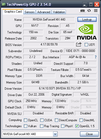