The most recent flagship model, the Intel Core i9-14900K
Intel Core is a line of multi-core (with the exception of Core Solo and Core 2 Solo) central processing units (CPUs) for midrange, embedded, workstation, high-end and enthusiast computer markets marketed by Intel Corporation. These processors displaced the existing mid- to high-end Pentium processors at the time of their introduction, moving the Pentium to the entry level. Identical or more capable versions of Core processors are also sold as Xeon processors for the server and workstation markets.
The lineup of Core processors includes the low-end Core i3, mid-end Core i5, high-end Core i7, and enthusiast Core i9 series.
In 2023, Intel announced that it would drop the "i" moniker from their processor branding, making it "Core 3/5/7/9". The company would introduce the "Ultra" branding for high-end processors as well.[1] The new naming scheme debuted with the launch of Raptor Lake-U Refresh and Meteor Lake processors in 2024, using the "Core 3/5/7" branding for mainstream processors and "Core Ultra 5/7/9" branding for "premium" high-end processors.[2][3]
Overview
Although Intel Core is a brand that promises no internal consistency or continuity, the processors within this family have been, for the most part, broadly similar.
The first products receiving this designation were the Core Solo and Core Duo Yonah processors for mobile from the Pentium M design tree, fabricated at 65nm and brought to market in January 2006. These are substantially different in design than the rest of the Intel Core product group, having derived from the Pentium Pro lineage that predated Pentium 4.
The first Intel Core desktop processor—and typical family member—came from the Conroe iteration, a 65nm dual-core design brought to market in July 2006, based on the Intel Core microarchitecture with substantial enhancements in micro-architectural efficiency and performance, outperforming Pentium 4 across the board (or near to it), while operating at drastically lower clock rates. Maintaining high instructions per cycle (IPC) on a deeply pipelined and resourced out-of-order execution engine has remained a constant fixture of the Intel Core product group ever since.
The new substantial bump in microarchitecture came with the introduction of the 45nm Bloomfield desktop processor in November 2008 on the Nehalem architecture, whose main advantage came from redesigned I/O and memory systems featuring the new Intel QuickPath Interconnect and an integrated memory controller supporting up to three channels of DDR3 memory.
Subsequent performance improvements have tended toward making additions rather than profound changes, such as adding the Advanced Vector Extensions (AVX) instruction set extensions to Sandy Bridge, first released on 32nm in January 2011. Time has also brought improved support for virtualization and a trend toward higher levels of system integration and management functionality (and along with that, increased performance) through the ongoing evolution of facilities such as Intel Active Management Technology (iAMT).
Since 2019, the Core brand has been based on four product lines, consisting of the entry level i3, the mainstream i5, the high-end i7, and the "enthusiast" i9.
In 2023, Intel announced that it would drop the "i" moniker from their processor branding, making it "Core 3/5/7/9". The company would introduce the "Ultra" branding for high-end processors as well.[1] The new naming scheme debuted with the launch of Raptor Lake-U Refresh and Meteor Lake processors in 2024, using the "Core 3/5/7" branding for mainstream processors and "Core Ultra 5/7/9" branding for "premium" high-end processors.[2][3]
January 2010 February 2011 June 2012 June 2013 January 2015 Sept. 2015 & June 2016 August 2016 November 2016 Jan. & June 2017 April 2018 May 2018 July 2018 August 2018 May & Aug. 2019 September 2019 Sept. 2020, Jan. - May 2021 January 2022
September 2009 January 2010 January 2011 February 2011 April 2012 June 2013 June 2015 September 2015 January 2017 October 2017 Oct. 2018 & Jan. 2019 April 2020 March 2021 Nov. 2021 & Jan. 2022
January 2010 February 2011 May 2012 June 2013 January 2015 September 2015 August 2016 January 2017 October 2017 April 2018 Aug. 2018 & Oct. 2018 Aug. 2018 & April 2019 May & Aug. 2019 September 2019 April 2020 Sept. 2020 - May 2021 January - September 2021 January 2022 January & May 2022
November 2008 September 2009 July 2010 January 2011 November 2011 February 2012 April 2012 June 2013 September 2013 June 2015 August 2015 January 2017 October 2017 October 2018 April 2020 March 2021 Nov. 2021 & Jan. 2022
September 2009 January 2010 January 2011 February 2011 May 2012 June 2013 January 2015 June 2015 September 2015 August 2016 January 2017 April 2018 August 2018 Aug. 2018 & April 2019 May & Aug. 2019 September 2019 April 2020 September 2020 January - September 2021 January 2022 January & May 2022
The original Core brand refers to Intel's 32-bit mobile dual-corex86CPUs, which derived from the Pentium M branded processors. The processor family used an enhanced version of the Intel P6 microarchitecture. It emerged in parallel with the NetBurst microarchitecture (Intel P68) of the Pentium 4 brand, and was a precursor of the 64-bit Core microarchitecture of Core 2 branded CPUs. The Core brand had two branches: the Duo (dual-core) and Solo (Duo with one disabled core, which replaced the Pentium M brand of single-core mobile processor). Intel launched the Core brand on January 6, 2006, with the release of the 32-bitYonahCPU–Intel's first dual-core mobile (low-power) processor. Its dual-core layout closely resembled two interconnected Pentium M branded CPUs packaged as a single die (piece) silicon chip (IC). Hence, the 32-bit microarchitecture of Core branded CPUs–contrary to its name–had more in common with Pentium M branded CPUs than with the subsequent 64-bit Core microarchitecture of Core 2 branded CPUs. Despite a major rebranding effort starting January 2006, some companies continued to market computers with the Yonah core marked as Pentium M. The Core series is also the first Intel processor used as the main CPU in an Apple Macintosh computer. The Core Duo was the CPU for the first generation MacBook Pro, while the Core Solo appeared in Apple's Mac Mini line. Core Duo signified the beginning of Apple's shift to Intel processors across the entire Mac line. In 2007, Intel began branding the Yonah core CPUs intended for mainstream mobile computers as Pentium Dual-Core, not to be confused with the desktop 64-bit Core microarchitecture CPUs also branded as Pentium Dual-Core. September 2007 and January 4, 2008, marked the discontinuation of a number of Core branded CPUs including several Core Solo, Core Duo, Celeron and one Core 2 Quad chip.[19][20]
Intel Core Solo[21] uses the same two-core die as the Core Duo, but features only one active core. Depending on demand, Intel may also simply disable one of the cores to sell the chip at the Core Solo price—this requires less effort than launching and maintaining a separate line of CPUs that physically only have one core. Intel had used the same strategy previously with the 486 CPU in which early 486SX CPUs were in fact manufactured as 486DX CPUs but with the FPU disabled. Intel Core Duo[22] consists of two cores on one die, a 2MB L2 cache shared by both cores, and an arbiter bus that controls both L2 cache and FSB (front-side bus) access.
The successor to Core is the mobile version of the Intel Core 2 line of processors using cores based upon the Intel Core microarchitecture,[23] released on July 27, 2006. The release of the mobile version of Intel Core 2 marks the reunification of Intel's desktop and mobile product lines as Core 2 processors were released for desktops and notebooks, unlike the first Intel Core CPUs that were targeted only for notebooks (although some small form factor and all-in-one desktops, like the iMac and the Mac Mini, also used Core processors).
Unlike the original Core, Intel Core 2 is a 64-bit processor, supporting Intel Extended Memory 64 Technology (EM64T). Another difference between the original Core Duo and the new Core 2 Duo is an increase in the amount of level 2 cache. The new Core 2 Duo has tripled the amount of on-board cache to 6MB. Core 2 also introduced a quad-core performance variant to the single- and dual-core chips, branded Core 2 Quad, as well as an enthusiast variant, Core 2 Extreme. All three chips are manufactured at a 65nm lithography, and in 2008, a 45nm lithography and support front side bus speeds ranging from 533MT/s to 1.6GT/s. In addition, the 45nm die shrink of the Core microarchitecture adds SSE4.1 support to all Core 2 microprocessors manufactured at a 45nm lithography, therefore increasing the calculation rate of the processors.
Core 2 Solo
The Core 2 Solo,[24] introduced in September 2007, is the successor to the Core Solo and is available only as an ultra-low-power mobile processor with 5.5 Watt thermal design power. The original U2xxx series "Merom-L" used a special version of the Merom chip with CPUID number 10661 (model 22, stepping A1) that only had a single core and was also used in some Celeron processors. The later SU3xxx are part of Intel's CULV range of processors in a smaller μFC-BGA 956 package but contain the same Penryn chip as the dual-core variants, with one of the cores disabled during manufacturing.
The majority of the desktop and mobile Core 2 processor variants are Core 2 Duo[25][26] with two processor cores on a single Merom, Conroe, Allendale, Penryn, or Wolfdale chip. These come in a wide range of performance and power consumption, starting with the relatively slow ultra-low-power Uxxxx (10W) and low-power Lxxxx (17W) versions, to the more performance oriented Pxxxx (25W) and Txxxx (35W) mobile versions and the Exxxx (65W) desktop models. The mobile Core 2 Duo processors with an 'S' prefix in the name are produced in a smaller μFC-BGA 956 package, which allows building more compact laptops.
Within each line, a higher number usually refers to a better performance, which depends largely on core and front-side bus clock frequency and amount of second level cache, which are model-specific. Core 2 Duo processors typically use the full L2 cache of 2, 3, 4, or 6MB available in the specific stepping of the chip, while versions with the amount of cache reduced during manufacturing are sold for the low-end consumer market as Celeron or Pentium Dual-Core processors. Like those processors, some low-end Core 2 Duo models disable features such as Intel Virtualization Technology.
Core 2 Quad[27][28] processors are multi-chip modules consisting of two dies similar to those used in Core 2 Duo, forming a quad-core processor. This allows twice the performance of a dual-core processors at the same clock frequency in ideal conditions.
Initially, all Core 2 Quad models were versions of Core 2 Duo desktop processors, Kentsfield derived from Conroe and Yorkfield from Wolfdale, but later Penryn-QC was added as a high-end version of the mobile dual-core Penryn.
The Xeon 32xx and 33xx processors are mostly identical versions of the desktop Core 2 Quad processors and can be used interchangeably.
Core 2 Extreme processors[29][30] are enthusiast versions of Core 2 Duo and Core 2 Quad processors, usually with a higher clock frequency and an unlocked clock multiplier, which makes them especially attractive for overclocking. This is similar to earlier Pentium D processors labeled as Extreme Edition. Core 2 Extreme processors were released at a much higher price than their regular version, often $999 or more.
With the release of the Nehalem microarchitecture in November 2008,[31] Intel introduced a new naming scheme for its Core processors. There are three variants, Core i3, Core i5 and Core i7, but the names no longer correspond to specific technical features like the number of cores. Instead, the brand is now divided from low-level (i3), through mid-range (i5) to high-end performance (i7),[32] which correspond to three, four and five stars in Intel's Intel Processor Rating[33] following on from the entry-level Celeron (one star) and Pentium (two stars) processors.[34] Common features of all Nehalem based processors include an integrated DDR3 memory controller as well as QuickPath Interconnect or PCI Express and Direct Media Interface on the processor replacing the aging quad-pumped Front Side Bus used in all earlier Core processors. All these processors have 256KB L2 cache per core, plus up to 12MB shared L3 cache. Because of the new I/O interconnect, chipsets and mainboards from previous generations can no longer be used with Nehalem-based processors.
Intel intended the Core i3 as the new low end of the performance processor line, following the retirement of the Core 2 brand.[35][36] The first Core i3 processors were launched on January 7, 2010.[37] The first Nehalem based Core i3 was Clarkdale-based, with an integrated GPU and two cores.[38] The same processor is also available as Core i5 and Pentium, with slightly different configurations. The Core i3-3xxM processors are based on Arrandale, the mobile version of the Clarkdale desktop processor. They are similar to the Core i5-4xx series but running at lower clock speeds and without Turbo Boost.[39] According to an Intel FAQ they do not support Error Correction Code (ECC) memory.[40] According to motherboard manufacturer Supermicro, if a Core i3 processor is used with a server chipset platform such as Intel 3400/3420/3450, the CPU supports ECC with UDIMM.[41] When asked, Intel confirmed that, although the Intel 5 series chipset supports non-ECC memory only with the Core i5 or i3 processors, using those processors on a motherboard with 3400 series chipsets it supports the ECC function of ECC memory.[42] A limited number of motherboards by other companies also support ECC with Intel Core ix processors; the Asus P8B WS is an example, but it does not support ECC memory under Windows non-server operating systems.[43]
Lynnfield was the first Core i5 processors using the Nehalem microarchitecture, introduced on September 8, 2009, as a mainstream variant of the earlier Core i7.[44][45] Lynnfield Core i5 processors have an 8MB L3 cache, a DMI bus running at 2.5GT/s and support for dual-channel DDR3-800/1066/1333 memory and have Hyper-threading disabled. The same processors with different sets of features (Hyper-threading and other clock frequencies) enabled are sold as Core i7-8xx and Xeon 3400-series processors, which should not be confused with high-end Core i7-9xx and Xeon W3500-series processors based on Bloomfield. A new feature called Turbo Boost Technology was introduced which maximizes speed for demanding applications, dynamically accelerating performance to match the workload. After Nehalem received a 32nm Westmere die shrink, Arrandale, the dual-core mobile Core i5 processors and its desktop counterpart Clarkdale was introduced in January 2010, together with Core i7-6xx and Core i3-3xx processors based on the same architecture. Arrandale processors have integrated graphics capability. Core i3-3xx does not support for Turbo Boost, L3 cache in Core i5-5xx processors is reduced to 3MB, while the Core i5-6xx uses the full cache,[46] Clarkdale is sold as Core i5-6xx, along with related Core i3 and Pentium processors. It has Hyper-Threading enabled and the full 4MB L3 cache.[47] According to Intel "Core i5 desktop processors and desktop boards typically do not support ECC memory",[48] but information on limited ECC support in the Core i3 section also applies to Core i5 and i7.[citation needed]
Intel Core i7 as a brand name applies to several families of desktop and laptop 64-bitx86-64 processors using the Nehalem, Westmere, Sandy Bridge, Ivy Bridge, Haswell, Broadwell, Skylake, and Kaby Lakemicroarchitectures. The Core i7 brand targets the business and high-end consumer markets for both desktop and laptop computers,[49] and is distinguished from the Core i3 (entry-level consumer), Core i5 (mainstream consumer), and Xeon (server and workstation) brands. Introduced in late 2008, Bloomfield was the first Core i7 processors based on the Nehalem architecture.[50][51][52][53] The following year, Lynnfield desktop processors and Clarksfield mobile processors brought new quad-core Core i7 models based on the said architecture.[54] After Nehalem received a 32nm Westmere die shrink, Arrandale dual-core mobile processors were introduced in January 2010, followed by Core i7's first six-core desktop processor Gulftown on March 16, 2010. Both the regular Core i7 and the Extreme Edition are advertised as five stars in the Intel Processor Rating. The first-generation Core i7 uses two different sockets; LGA 1366 designed for high-end desktops and servers, and LGA 1156 used in low- and mid-end desktops and servers. In each generation, the highest-performing Core i7 processors use the same socket and QPI-based architecture as the medium-end Xeon processors of that generation, while lower-performing Core i7 processors use the same socket and PCIe/DMI/FDI architecture as the Core i5. "Core i7" is a successor to the Intel Core 2 brand.[55][56][57][58] Intel representatives stated that they intended the monikerCore i7 to help consumers decide which processor to purchase as Intel releases newer Nehalem-based products in the future.[59]
↑ Price reflects Recommended Customer Price (RCP) rather than MSRP. RCP is the cost per unit, in bulk sales of 1000 units or more, to OEMs, ODMs, and retail outlets when purchasing from Intel. Actual MSRP is higher than RCP
In early 2011, Intel introduced a new microarchitecture named Sandy Bridge. This is the second generation of the Core processor microarchitecture. It kept all the existing brands from Nehalem, including Core i3/i5/i7, and introduced new model numbers. The initial set of Sandy Bridge processors includes dual- and quad-core variants, all of which use a single 32nm die for both the CPU and integrated GPU cores, unlike the earlier microarchitectures. All Core i3/i5/i7 processors with the Sandy Bridge microarchitecture have a four-digit model number. With the mobile version, the thermal design power can no longer be determined from a one- or two-letter suffix but is encoded into the CPU number. Starting with Sandy Bridge, Intel no longer distinguishes the code names of the processor based on number of cores, socket or intended usage; they all use the same code name as the microarchitecture itself.
Ivy Bridge is the codename for Intel's 22nm die shrink of the Sandy Bridge microarchitecture based on tri-gate ("3D") transistors, introduced in April 2012.
Core i3
Released on January 20, 2011, the Core i3-2xxx line of desktop and mobile processors is a direct replacement of the 2010 "Clarkdale" Core i3-5xx and "Arrandale" Core i3-3xxM models, based on the new microarchitecture. While they require new sockets and chipsets, the user-visible features of the Core i3 are largely unchanged, including the lack of support for Turbo Boost and AES-NI. Unlike the Sandy Bridge-based Celeron and Pentium processors, the Core i3 line does support the new Advanced Vector Extensions. This particular processor is the entry-level processor of this new series of Intel processors.
A Core i5-2500K. The K suffix indicates an unlocked clock multiplier, which allows for easier overclocking.
In January 2011, Intel released new quad-core Core i5 processors based on the "Sandy Bridge" microarchitecture at CES 2011. New dual-core mobile processors and desktop processors arrived in February 2011.
The Core i5-2xxx line of desktop processors are mostly quad-core chips, with the exception of the dual-core Core i5-2390T, and include integrated graphics, combining the key features of the earlier Core i5-6xx and Core i5-7xx lines. The suffix after the four-digit model number designates unlocked multiplier (K), low-power (S) and ultra-low-power (T).
The desktop CPUs now all have four non-SMT cores (like the i5-750), with the exception of the i5-2390T. The DMI bus runs at 5GT/s.
The mobile Core i5-2xxxM processors are all dual-core and hyper-threaded chips like the previous Core i5-5xxM series, and share most of the features with that product line.
The Core i7 brand was the high-end for Intel's desktop and mobile processors, until the announcement of the i9 in 2017. Its Sandy Bridge models feature the largest amount of L3 cache and the highest clock frequency. Most of these models are very similar to their smaller Core i5 siblings. The quad-core mobile Core i7-2xxxQM/XM processors follow the previous "Clarksfield" Core i7-xxxQM/XM processors, but now also include integrated graphics.
Ivy Bridge is the codename for a "third generation" line of processors based on the 22nm manufacturing process developed by Intel. Mobile versions of the CPU were released in April 2012 following with desktop versions in September 2012.
This section needs expansion. You can help by adding to it. (April 2014)
Core i3
This section needs expansion. You can help by adding to it. (April 2014)
The Ivy Bridge-based Core-i3-3xxx line is a minor upgrade to 22nm process technology and better graphics.
Broadwell is the fifth generation Core processor microarchitecture, and was released by Intel on September 6, 2014, and began shipping in late 2014. It is the first to use a 14nm chip.[68] Additionally, mobile processors were launched in January 2015[69] and Desktop Core i5 and i7 processors were released in June 2015.[70]
Skylake is the sixth generation Core processor microarchitecture, and was launched in August 2015. Being the successor to the Broadwell line, it is a redesign using the same 14nm manufacturing process technology; however the redesign has better CPU and GPU performance and reduced power consumption. Intel also disabled overclocking non -K processors.
This section needs expansion. You can help by adding to it. (January 2017)
Kaby Lake is the codename for the seventh generation Core processor, and was launched in October 2016 (mobile chips)[71] and January 2017 (desktop chips).[72] With the latest generation of microarchitecture, Intel decided to produce Kaby Lake processors without using their "tick–tock" manufacturing and design model.[73] Kaby Lake features the same Skylake microarchitecture and is fabricated using Intel's 14 nanometer manufacturing process technology.[73]
Built on an improved 14nm process (14FF+), Kaby Lake features faster CPU clock speeds and Turbo frequencies. Beyond these process and clock speed changes, little of the CPU architecture has changed from Skylake, resulting in identical IPC.
Kaby Lake features a new graphics architecture to improve performance in 3D graphics and 4K video playback. It adds native High-bandwidth Digital Content Protection 2.2 support, along with fixed function decode of H.264/MPEG-4 AVC, High Efficiency Video Coding Main and Main10/10-bit, and VP9 10-bit and 8-bit video. Hardware encode is supported for H.264/MPEG-4 AVC, HEVC Main10/10-bit, and VP9 8-bit video. VP9 10-bit encode is not supported in hardware. OpenCL 2.1 is now supported.
Kaby Lake is the first Core architecture to support hyper-threading for the Pentium-branded desktop CPU SKU. Kaby Lake also features the first overclocking-enabled i3-branded CPU.
Kaby Lake-X processors are modified versions of Kaby Lake-S processors that fit into the LGA 2066 socket. However, they can't take advantage of the unique features of the platform.
Coffee Lake is a codename for the eighth generation Intel Core family and was launched in October 2017. For the first time in the ten-year history of Intel Core processors, the Coffee Lake generation features an increase in core counts across the desktop lineup of processors, a significant driver of improved performance versus previous generations despite similar per-clock performance.
Increase in number of CPU cores in desktop Coffee Lake processors
Kaby Lake (7th Generation)
Coffee Lake (8th Generation)
Cores / Threads
Cores / Threads
Core i3
2 / 40
4 / 40
Core i5
4 / 40
6 / 60
Core i7
4 / 80
6 / 12
* Intel Hyper-threading capabilities allow an enabled processor to execute two threads per physical core
Coffee Lake features largely the same CPU core and performance per MHz as Skylake/Kaby Lake.[74][75] Features specific to Coffee Lake include:
Following similar refinements to the 14nm process in Skylake and Kaby Lake, Coffee Lake is the third 14nm process refinement ("14nm++") and features increased transistor gate pitch for a lower current density and higher leakage transistors which allows higher peak power and higher frequency at the expense of die area and idle power.
Coffee Lake will be used in conjunction with the 300-series chipset and is incompatible with the older 100- and 200-series chipsets.[76][77]
Increased L3 cache in accordance to the number of cores
Increased turbo clock speeds across i5 and i7 CPUs models (increased by up to 200MHz)
Increased iGPU clock speeds by 50MHz
DDR4 memory support updated for 2666MHz (for i5 and i7 parts) and 2400MHz (for i3 parts); DDR3 memory is no longer supported
Whiskey Lake is Intel's codename for the third 14nm Skylake process-refinement, following Kaby Lake Refresh and Coffee Lake. Intel announced low power mobile Whiskey Lake CPUs availability on August 28, 2018.[79][80] It has not yet been advertised whether this CPU architecture contains hardware mitigations for Meltdown/Spectre class vulnerabilities—various sources contain conflicting information.[81][82][80][83] Unofficially it was announced that Whiskey Lake has hardware mitigations against Meltdown and L1TF while Spectre V2 requires software mitigations as well as microcode/firmware update.[84][85][86][87]
Architecture changes compared to Kaby Lake Refresh
Cannon Lake (formerly Skymont) is Intel's codename for the 10-nanometerdie shrink of the Kaby Lakemicroarchitecture. As a die shrink, Cannon Lake is a new process in Intel's "process–architecture–optimization" execution plan as the next step in semiconductor fabrication.[88] Cannon Lake are the first mainstream CPUs to include the AVX-512 instruction set. In comparison to the previous generation AVX2 (AVX-256), the new generation AVX-512 most notably provides double the width of data registers and double the number of registers. These enhancements would allow for twice the number of floating point operations per register due to the increased width in addition to doubling the overall number of registers, resulting in theoretical performance improvements of up to four times the performance of AVX2.[89][90]
At CES 2018, Intel announced that they had started shipping mobile Cannon Lake CPUs at the end of 2017 and that they would ramp up production in 2018.[91][92][93] No further details were disclosed.
Cascade Lake X-Series CPUs are the 10th generation versions of the previous Skylake X-Series CPUs. They offer minor clockspeed improvements and a highly reduced price.
Ice Lake is codename for Intel's 10th generation Intel Core processors, representing an enhancement of the 'architecture' of the preceding generation Kaby Lake/Cannon Lake processors (as specified in Intel's process–architecture–optimization execution plan). As the successor to Cannon Lake, Ice Lake uses Intel's newer 10nm+ fabrication process, and is powered by the Sunny Cove microarchitecture.
Comet Lake is Intel's codename for the fourth 14nm Skylake process-refinement, following Whiskey Lake. Intel announced low power mobile Comet Lake CPUs availability on August 21, 2019.[116]
Architecture changes in Comet Lake-U compared to Whiskey Lake
AVX/AVX2 instructions support for Pentium Gold and Celeron processors has been unlocked
GPU
Intel Xe-LP ("Gen12") GPU with up to 96 execution units[126] (50% uplift compared to Ice Lake) with some yet to be announced processors using Intel's discrete GPU, DG1[127][128]
LPDDR5-5400 "architecture capability" (Intel expects Tiger Lake products with LPDDR5 to be available around Q1 2021)[136][137][138] Designs with LPDDR5 memory are yet to be announced as of March 2022.
Miniaturization of CPU and motherboard into an M.2SSD-sized small circuit board[127]
Mobile processors (Tiger Lake-H)
All models support DDR4-3200 memory
All models support 20 reconfigurable PCI Express 4.0 lanes, allowing x16 Gen 4 link for discrete GPU and x4 Gen 4 link for M.2 SSDs
Rocket Lake is a codename for Intel's desktop x86 chip family based on the new Cypress Cove microarchitecture, a variant of Sunny Cove (used by Intel's Ice Lake mobile processors) backported to the older 14nm process.[140] The chips are marketed as "Intel 11th generation Core". Launched March 30, 2021.
Architecture changes in comparison with Comet Lake
All CPUs listed below support DDR4-3200 natively. The Core i9 K/KF processors enable a 1:1 ratio of DRAM to memory controller by default at DDR4-3200, whereas the Core i9 non K/KF and all other CPUs listed below enable a 2:1 ratio of DRAM to memory controller by default at DDR4-3200 and a 1:1 ratio by default at DDR4-2933.[152]
Alder Lake is Intel's codename for the 12th generation of Intel Core processors based on a hybrid architecture utilizing Golden Cove high-performance cores and Gracemont power-efficient cores.[153] It is fabricated using Intel's Intel 7 process, previously referred to as Intel 10nm Enhanced SuperFin (10ESF). Intel officially announced 12th Gen Intel Core CPUs on October 27, 2021, and was launched to the market on November 4, 2021.[154]
New 6-wide instruction decoder (up from 4-wide in Rocket Lake/Tiger Lake) with the ability to fetch up to 32 bytes of instructions per cycle (up from 16)[155]
12 execution ports (up from 10)
512 reorder-buffer entries (up from 384)
6-wide μOP allocations (up from 5)
μOP cache size increased to 4K entries (up from 2.25K)
AVX-512 (including FP16) is present but disabled by default to match E-cores. It still can be enabled on some motherboards by disabling the E-cores[155][156]
Intel Thread Director / Hardware Feedback Interface (HFI),[159][160] a hardware technology to assist the OS thread scheduler with more efficient load distribution between heterogeneous CPU cores.[137] Enabling this new capability requires support in operating systems. Microsoft added support for Thread Director to Windows 11,[155][161] while support to Linux was merged in kernel 5.18.[160][162]
By default Alder Lake CPUs are configured to run at Turbo Power at all times and Base Power is only guaranteed when P-Cores/E-cores do not exceed the base clock rate.[155]
Max Turbo Power: the maximum sustained (>1s) power dissipation of the processor as limited by current and/or temperature controls. Instantaneous power may exceed Maximum Turbo Power for short durations (≤10ms). Maximum Turbo Power is configurable by system vendor and can be system specific.
CPUs in bold below feature ECC memory support only when paired with a motherboard based on the W680 chipset.[167]
*By default, Core i9 12900KS achieves 5.5GHz only when using Thermal Velocity Boost[168]
Raptor Lake is Intel's codename for the 13th generation of Intel Core processors and the second generation based on a hybrid architecture.[170] It is fabricated using an improved version of Intel's Intel 7 process.[171] Intel launched Raptor Lake on October 22, 2022.
Raptor Lake Refresh is Intel's codename for the 14th generation of Intel Core processors. It is a refresh and based on the same architecture of the 13th generation with clock speeds of up to 6.2GHz on the Core i9 14900KS, 6GHz on the Core i9 14900K and 14900KF, 5.6GHz on the Core i7 14700K and 14700KF, and 5.3GHz on the Core i5 14600K and 13400KF as well as UHD Graphics 770 on non-F processors. They are still based on the Intel 7 process node.[176] Introduced on October 17, 2023, these CPUs are designed for the LGA 1700 socket, which allows for compatibility with 600 and 700 series motherboards.[177] It is the last generation CPUs to use the Intel Core i3, i5, i7 and i9 naming scheme as Intel announced that they will be dropping the "i" prefix for future Intel Core processors in 2023.[1]
The 14th generation CPU does not feature any major architectural changes over Raptor Lake, but does feature some minor improvements.[178] The 14th generation CPU is widely criticized as a last-ditch effort to beat AMD's Zen 4 with X3D V-Cache[179][180] as Intel's desktop version of the next generation architecture, Meteor Lake, was cancelled and the Arrow Lake architecture was not yet ready for release.[181]
Architecture comparison to 13th generation desktop[176][178]
Same LGA 1700 socket
600 and 700 series chipsets require a BIOS update to support 14th generation CPU.
Same DDR4 and DDR5 support
DDR4-3200
DDR5-5600
Increased E-core count on i7s when compared to 13700K (added four E-cores)
Reception
This section needs expansion. You can help by adding to it. (January 2023)
Vulnerabilities
In early 2018, news reports indicated that the security flaws Meltdown and Spectre were found "in virtually all Intel processors [made in the past two decades] that will require fixes within Windows, macOS and Linux". The flaw also affected cloud servers. At the time, Intel was not commenting on this issue.[182][183] According to a New York Times report, "There is no easy fix for Spectre ... as for Meltdown, the software patch needed to fix the issue could slow down computers by as much as 30 percent".[184]
In mid 2018, the majority of Intel Core processors were found to possess a defect (the Foreshadow vulnerability), which undermines the Software Guard Extensions (SGX) feature of the processor.[185][186][187]
In March 2020, computer security experts reported another Intel chip security flaw, besides the Meltdown and Spectre flaws, with the systematic name CVE-2019-0090 (or, "Intel CSME Bug", referencing the Converged Security and Management Engine). This newly found flaw is not fixable with a firmware update, and affects nearly "all Intel chips released in the past five years".[188][189][190]
Xeon is a brand of x86 microprocessors designed, manufactured, and marketed by Intel, targeted at the non-consumer workstation, server, and embedded markets. It was introduced in June 1998. Xeon processors are based on the same architecture as regular desktop-grade CPUs, but have advanced features such as support for error correction code (ECC) memory, higher core counts, more PCI Express lanes, support for larger amounts of RAM, larger cache memory and extra provision for enterprise-grade reliability, availability and serviceability (RAS) features responsible for handling hardware exceptions through the Machine Check Architecture (MCA). They are often capable of safely continuing execution where a normal processor cannot due to these extra RAS features, depending on the type and severity of the machine-check exception (MCE). Some also support multi-socket systems with two, four, or eight sockets through use of the Ultra Path Interconnect (UPI) bus, which replaced the older QuickPath Interconnect (QPI) bus.
As of 2020, the x86 architecture is used in most high end compute-intensive computers, including cloud computing, servers, workstations, and many less powerful computers, including personal computer desktops and laptops. The ARM architecture is used in most other product categories, especially high-volume battery powered mobile devices such as smartphones and tablet computers.
Intel Core 2 was a processor family encompassing a range of Intel's mainstream 64-bit x86-64 single-, dual-, and quad-core microprocessors based on the Core microarchitecture. The single- and dual-core models are single-die, whereas the quad-core models comprise two dies, each containing two cores, packaged in a multi-chip module. The Core 2 range was the last flagship range of Intel desktop processors to use a front-side bus (FSB).
Pentium is a discontinued series of x86 architecture-compatible microprocessors produced by Intel. The original Pentium was first released on March 22, 1993. The name "Pentium" is originally derived from the Greek word pente (πεντε), meaning "five", a reference to the prior numeric naming convention of Intel's 80x86 processors (8086–80486), with the Latin ending -ium since the processor would otherwise have been named 80586 using that convention.
Sandy Bridge is the codename for Intel's 32 nm microarchitecture used in the second generation of the Intel Core processors. The Sandy Bridge microarchitecture is the successor to Nehalem and Westmere microarchitecture. Intel demonstrated an A1 stepping Sandy Bridge processor in 2009 during Intel Developer Forum (IDF), and released first products based on the architecture in January 2011 under the Core brand.
Tick–tock was a production model adopted in 2007 by chip manufacturer Intel. Under this model, every microarchitecture change (tock) was followed by a die shrink of the process technology (tick). It was replaced by the process–architecture–optimization model, which was announced in 2016 and is like a tick–tock cycle followed by an optimization phase. As a general engineering model, tick–tock is a model that refreshes one side of a binary system each release cycle.
Haswell is the codename for a processor microarchitecture developed by Intel as the "fourth-generation core" successor to the Ivy Bridge. Intel officially announced CPUs based on this microarchitecture on June 4, 2013, at Computex Taipei 2013, while a working Haswell chip was demonstrated at the 2011 Intel Developer Forum. Haswell was the last generation of Intel processor to have socketed processors on mobile. With Haswell, which uses a 22 nm process, Intel also introduced low-power processors designed for convertible or "hybrid" ultrabooks, designated by the "U" suffix. Haswell began shipping to manufacturers and OEMs in mid-2013, with its desktop chips officially launched in September 2013.
Arrandale is the code name for a family of mobile Intel processors, sold as mobile Intel Core i3, i5 and i7 as well as Celeron and Pentium. It is closely related to the desktop Clarkdale processor; both use dual-core dies based on the Westmere 32 nm die shrink of the Nehalem microarchitecture, and have integrated Graphics as well as PCI Express and DMI links.
Clarkdale is the codename for Intel's first-generation Core i5, i3 and Pentium dual-core desktop processors. It is closely related to the mobile Arrandale processor; both use dual-core dies based on the 32 nm Westmere microarchitecture and have integrated Graphics, PCI Express and DMI links built-in.
Skylake is Intel's codename for its sixth generation Core microprocessor family that was launched on August 5, 2015, succeeding the Broadwell microarchitecture. Skylake is a microarchitecture redesign using the same 14 nm manufacturing process technology as its predecessor, serving as a tock in Intel's tick–tock manufacturing and design model. According to Intel, the redesign brings greater CPU and GPU performance and reduced power consumption. Skylake CPUs share their microarchitecture with Kaby Lake, Coffee Lake, Whiskey Lake, and Comet Lake CPUs.
LGA 1151, also known as Socket H4, is a type of zero insertion force flip-chip land grid array (LGA) socket for Intel desktop processors which comes in two distinct versions: the first revision which supports both Intel's Skylake and Kaby Lake CPUs, and the second revision which supports Coffee Lake CPUs exclusively.
Kaby Lake is Intel's codename for its seventh generation Core microprocessor family announced on August 30, 2016. Like the preceding Skylake, Kaby Lake is produced using a 14 nanometer manufacturing process technology. Breaking with Intel's previous "tick–tock" manufacturing and design model, Kaby Lake represents the optimized step of the newer process–architecture–optimization model. Kaby Lake began shipping to manufacturers and OEMs in the second quarter of 2016, with its desktop chips officially launched in January 2017.
Ice Lake is Intel's codename for the 10th generation Intel Core mobile and 3rd generation Xeon Scalable server processors based on the Sunny Cove microarchitecture. Ice Lake represents an Architecture step in Intel's process–architecture–optimization model. Produced on the second generation of Intel's 10 nm process, 10 nm+, Ice Lake is Intel's second microarchitecture to be manufactured on the 10 nm process, following the limited launch of Cannon Lake in 2018. However, Intel altered their naming scheme in 2020 for the 10 nm process. In this new naming scheme, Ice Lake's manufacturing process is called simply 10 nm, without any appended pluses.
Coffee Lake is Intel's codename for its eighth-generation Core microprocessor family, announced on September 25, 2017. It is manufactured using Intel's second 14 nm process node refinement. Desktop Coffee Lake processors introduced i5 and i7 CPUs featuring six cores and Core i3 CPUs with four cores and no hyperthreading.
Comet Lake is Intel's codename for its 10th generation Core processors. They are manufactured using Intel's third 14 nm Skylake process revision, succeeding the Whiskey Lake U-series mobile processor and Coffee Lake desktop processor families. Intel announced low-power mobile Comet Lake-U CPUs on August 21, 2019, H-series mobile CPUs on April 2, 2020, desktop Comet Lake-S CPUs April 30, 2020, and Xeon W-1200 series workstation CPUs on May 13, 2020. Comet Lake processors and Ice Lake 10 nm processors are together branded as the Intel "10th Generation Core" family. Intel officially launched Comet Lake-Refresh CPUs on the same day as 11th Gen Core Rocket Lake launch. The low-power mobile Comet Lake-U Core and Celeron 5205U CPUs were discontinued on July 7, 2021.
Rocket Lake is Intel's codename for its 11th generation Core microprocessors. Released on March 30, 2021, it is based on the new Cypress Cove microarchitecture, a variant of Sunny Cove backported to Intel's 14 nm process node. Rocket Lake cores contain significantly more transistors than Skylake-derived Comet Lake cores.
Alder Lake is Intel's codename for the 12th generation of Intel Core processors based on a hybrid architecture utilizing Golden Cove performance cores and Gracemont efficient cores. It is fabricated using Intel's Intel 7 process, previously referred to as Intel 10 nm Enhanced SuperFin (10ESF). The 10ESF has a 10%-15% boost in performance over the 10SF used in the mobile Tiger Lake processors. Intel officially announced 12th Gen Intel Core CPUs on October 27, 2021, mobile CPUs and non-K series desktop CPUs on January 4, 2022, Alder Lake-P and -U series on February 23, 2022, and Alder Lake-HX series on May 10, 2022.
↑ Asus P8B WS specificationArchived September 25, 2011, at the Wayback Machine : supports "ECC, Non-ECC, un-buffered Memory", but "Non-ECC, un-buffered memory only support for client OS (Windows 7, Vista and XP)."
This page is based on this Wikipedia article Text is available under the CC BY-SA 4.0 license; additional terms may apply. Images, videos and audio are available under their respective licenses.
 Intel Core i3 logo
 Intel Core i5 logo
 Intel Core i7 logo
 Intel Core i9 logo
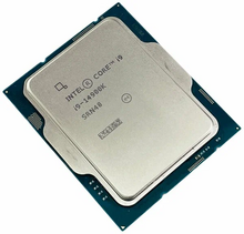


