Meteor Lake

Last updated

Meteor Lake
General information
LaunchedDecember 14, 2023 (2023-12-14) [1]
Marketed by Intel
Designed by Intel
Common manufacturer(s)
CPUID codeA06A4h
Product code80723 [2]
Performance
Max. CPU clock rate P-cores: 5.1 GHz
E-cores: 3.8 GHz
LP E-cores: 2.5 GHz
DMI speedsx8 16 GT/s
Cache
L1 cache 112 KB per P-core:
  • 64 KB instructions
  • 48 KB data

96 KB per E-core and LP E-core:
  • 64 KB instructions
  • 32 KB data
L2 cache2 MB per P-core, E-core cluster and LP E-core cluster
L3 cacheUp to 24 MB
Architecture and classification
ApplicationMobile
Technology node Intel 4 [3]
TSMC N5
TSMC N6
Intel 22FFL
Microarchitecture Redwood Cove (P-cores)
Crestmont (E-cores and LP E-cores)
Instruction set x86-64
Instructions x86-64
Extensions
Physical specifications
Cores
  • 2–6 P-cores
    8 E-cores
    2 LP E-cores
Memory (RAM)
  • Up to 96 GB
  • Up to dual-channel DDR5-5600 (expect 9 W models)
  • Up to dual-channel LPDDR5X-7467 (all models)
GPU(s) Intel Arc
Package(s)
Socket(s)
Products, models, variants
Product code name(s)
  • MTL
Model(s)
  • Meteor Lake-H
  • Meteor Lake-U
  • Meteor Lake-HL
  • Meteor Lake-UL
Brand name(s)
History
Predecessor(s) Alder Lake (embedded and 9 W fanless mobile)
Raptor Lake (15 W - 45 W premium fanned mobile)
Successor(s) Lunar Lake (low power ultralight)
Arrow Lake (performance thin & light)
Support status
Supported

Meteor Lake is Intel's codename for the first generation of Intel Core Ultra mobile processors, [4] and was officially launched on December 14, 2023. [5] It is the first generation of Intel mobile processors to use a chiplet architecture which means that the processor is a multi-chip module. [4] Tim Wilson led the system on a chip development for this generation microprocessor. [6]

Contents

Background

In July 2021, Meteor Lake was initially announced to be coming with a 5–125W TDP range for various segments ranging from ultra low power mobile to enthusiast desktop. [7] The initial tape-in process for Meteor Lake took place in May 2021. The CPU compute tile was confirmed to be fabricated on Intel's 7nm process (since rebranded to "Intel 4"). [8] [3]

In October 2021, Intel said in an earnings call that it had taped out the CPU compute tile for Meteor Lake and after it was received it had powered on within 30 minutes and with expected performance levels. [9] In April 2022, Intel announced that an assembled Meteor Lake mobile processor had been powered-on for the first time in a development milestone. [10] [11]

In March 2023, it was reported that Intel had decided to cancel development of high-end Meteor Lake-S processors for desktop. [12] Meteor Lake-S processors were being designed to fit into the LGA 1851 socket, which is identical in dimensions to LGA 1700, but the cancellation of desktop Meteor Lake meant that the LGA 1851 socket won't debut until Arrow Lake in 2024. [13] The top Meteor Lake-S SKU in development contained 6 Redwood Cove P-cores and 16 Crestmont E-cores, which is two fewer P-cores than the last generation Raptor Lake Core i9-13900K.

At Intel's Innovation event in September 2023, head of Intel's Client Computing Group Michelle Johnston Holthaus confirmed that some Meteor Lake-based processors would come to desktop in 2024. Intel later clarified that socketable desktop Meteor Lake processors would not be coming to the DIY market with the LGA 1851 socket. [14] [15] Instead, Meteor Lake processors in a BGA package will be available on desktop in the form of compact all-in-one PCs. [16] A reason for this, according to a statement by Intel to ComputerBase, is that "Meteor Lake is a power efficient architecture that will power innovative mobile and desktop designs". [17]

Branding

Intel unveiled new branding in June 2023 for upcoming Meteor Lake processors after using the same "Core i" branding for over 15 years. Core branding would be simplified by dropping the 'i' with processors branded Core 3, 5 and 7 instead. [18] The new 'Core Ultra' 5, 7 and 9 branding would be reserved for "premium" processors according to Intel. [19] In addition to the new tier naming, Intel said it would be de-emphasizing processor generations in marketing material, though the processor generation number would remain in the processor number. [20] Meteor Lake processors with Core Ultra branding are classified as first generation Core Ultra.

The new Core and Core Ultra branding was perceived as creating more branding confusion rather than reducing it. [21] Josh Loeffler of TechRadar wrote that "differentiation between Core and Core Ultra is also somewhat head-scratching, especially since there will at least be some overlap between the two brands" as Core 5 and Core 7 processors will exist alongside Core Ultra 5 and Core Ultra 7 processors. [22] In the view of Digital Trends , the new branding emulated AMD and Apple's naming conventions which amounted to Intel "chasing its competitors instead of leading the pack". [23]

Intel Core branding (2020–2023)
Intel Core i3 (11th generation, logo).svg
Core i3
Intel Core i5 (11th generation, logo).svg
Core i5
Intel Core i7 (11th generation, logo).svg
Core i7
Intel Core i9 (11th generation, logo).svg
Core i9
Intel Core and Core Ultra branding (since 2023)
Intel-Core-3-Badge-2023.png
Core 3
Intel-Core-5-Badge-2023.png
Core 5
Intel-Core-7-Badge-2023.png
Core 7
Intel-Core-Ultra-5-Badge-2023.png
Core Ultra 5
Intel-Core-Ultra-7-Badge-2023.png
Core Ultra 7
Intel-Core-Ultra-9-Badge-2023.png
Core Ultra 9

Production

Intel's production facility in Hillsboro, Oregon where the D1D fabrication facility is located (April 2009) Intel facility in Hillsboro, Oregon.jpg
Intel's production facility in Hillsboro, Oregon where the D1D fabrication facility is located (April 2009)

In April 2023, Meteor Lake and its "Intel 4" process were reportedly ramping to production. [24] Production on Meteor Lake with Intel 4 wafers took place at Intel's D1D fabrication facility in Hillsboro, Oregon. [25] The D1D fabrication facility has a total output of 40,000 wafers a month. [26] Secondary source production for Meteor Lake takes place at Fab 34 in the Republic of Ireland. [27] [28] On September 29, 2023, Intel announced that Intel 4 products, including Meteor Lake, had entered high-volume production at Fab 34 in the Republic of Ireland. [29] The GPU, SoC and I/O extender tiles in Meteor Lake are manufactured by TSMC in Taiwan.

Unveiling and release

Meteor Lake was revealed at Intel's Innovation event on September 19, 2023, with the announcement that 'Core Ultra' branded processors would be launching on December 14. [30] However, no list of Meteor Lake SKUs were revealed at Innovation nor release details on regular 'Core' branded processors. [31]

Architecture

Packaging

Meteor Lake is a 64-bit x86 CPU architecture designed around low power operation and increased power efficiency over Raptor Lake. It is the first Intel microarchitecture to utilize a disaggregated multi-chip module (MCM) approach rather than using large monolithic silicon dies. Previously, in June 2017, Intel had derided AMD's disaggregated chiplet approach in their Ryzen and Epyc processors as using "glued-together" dies. [32]

The first advantage of using smaller dies in an MCM is how it brings better modularity and fabricating smaller dies increases silicon yield rates as more dies can be fitted onto a single 300mm wafer. As a result of greater yields, the use of multiple pre-tested components in an MCM removes the need for binning an entire assembled CPU as is the case with monolithic dies. [33] For example, Raptor Lake desktop silicon with defective graphics is binned into F SKUs with the integrated graphics disabled so they can still be sold while non-F SKUs have their integrated graphics enabled. Instead, Intel can assemble Meteor Lake CPUs using multiple pieces of fully functional silicon while any silicon wafer defects can be discarded entirely. The second advantage is greater flexibility in the use of process nodes. The various dies in an MCM can be fabricated on different nodes depending on their use case. Certain functions like SRAM and general I/O do not linearly scale as logic does with advancements in process node. For example, an I/O die can use a cheaper, more mature process like TSMC's N6 while the CPU die can use a more expensive, advanced node like N5 or N3 for greater power efficiency and frequency.

Process technology

Due to its MCM construction, Meteor Lake can take advantage of different process nodes that are best suited to the use case. Meteor Lake is built using four different fabrication nodes, including both Intel's own nodes and external nodes outsourced to fabrication competitor TSMC. The "Intel 4" process used for the CPU tile is the first process node in which Intel is utilising extreme ultraviolet (EUV) lithography, which is necessary for creating nodes 7nm and smaller. The interposer base tile is fabricated on Intel's 22FFL, or "Intel 16", process. [34] [35] The 22FFL (FinFET Low-power) node, first announced in March 2017, was designed for inexpensive low power operation. [36] The interposer base tile is designed to connect tiles together and allow for die-to-die communciation which does not require the most advanced, expensive nodes so an older, inexpensive node can be used instead.

TileNodeEUVDie sizeRef.
Compute tile Intel 4 (7nm EUV)Yes check.svg69.67 mm2 [37]
[38]
[39]
Graphics tile TSMC N5 Yes check.svg44.25 mm2
SoC tile TSMC N6 Yes check.svg100.15 mm2
I/O extender tile TSMC N6 Yes check.svg27.42 mm2
Foveros interposer base tile Intel 16 (22FFL)Dark Red x.svg265.65 mm2

Compute tile

Meteor Lake's CPU compute tile features up to 6 Redwood Cove P-cores and 8 Crestmont E-cores. Each Redwood Cove P-core features SMT with two threads per core while Crestmont E-cores are limited to one thread per core. The 8 total Cresmont E-cores are organized into two 4-core clusters with shared L2 and L3 caches for each cluster. Each Crestmont E-core cluster has 2 MB of L2 cache, the same as a Gracemont E-core cluster. Crestmont maintais the same 6-wide out-of-order core design as Gracemont with enhancements to its pipeline. The branch target buffer in Cresmont gets a boost from 5120 entries to 6144 entries. [40] Intel claims that Cresmont achieves a 3% IPC increase due to the addition of Vector Neural Network Instructions (VNNI) instructions support for AI workloads but Cresmont E-cores still lack support for AVX-512 instructions. [41] Testing of Meteor Lake's new Redwood Cove P-cores actually showed an IPC regression in single-core workloads over the previous generation Raptor Cove core. [42]

Meteor Lake's compute tile is fabricated on the Intel 4 node which Intel claims brings brings a 20% increase in power efficiency and twice the area density for logic over Intel 7. [43] The CPU tile measures around 8.9mm × 8.3mm in dimensions, giving a total die size of 73.87mm2. [39] As a result, roughly 730 CPU dies can be fabricated from a single 300mm wafer, though the usable die yields will be lower than 730. [39]

Graphics tile

The dedicated graphics tile in Meteor Lake is fabricated using TSMC's N5 node. Contained within the graphics tile are up to 8 Xe-LPG graphics cores based on the Alchemist architecture with optimizations for low-power. Intel's Arc A-series discrete graphics cards use Xe-HPG cores that are also based on the same Alchemist architecture. Each Xe core has 16 Xe Vector Engines (XVEs), giving a total of 128 XVEs across the 8 Xe-LPG cores. This 128 XVE configuration is a downgrade from the 192 XVEs Intel originally showed for Meteor Lake's graphics in a July 2021 presentation slide. [7] The move to the Alchemist architecture also brings the addition of up to 8 ray tracing units, one in each Xe-LPG core. [44] Much like the Xe-HPG variant, each Xe-LPG core contains a 192 KB L1 cache shared between all 16 XVEs. The 8 Xe-LPG cores have access to a 4 MB global L2 cache. [45] However, what the graphics tile is missing from the Alchemist architecture are Xe Matrix Extensions (XMX) units. XMX units perform in-silicon AI acceleration, similar to Nvidia's Tensor cores. The lack of XMX units means that the Xe-LPG core instead uses DP4a instructions in line with Microsoft Shader Model 6.4. [46]

Meteor Lake's graphics capabilities are greatly increased over the previous generation UHD and Iris integrated graphics in Raptor Lake. Intel claims that Meteor Lake's GPU achieves a 2x increase in performance-per-watt over the Iris Xe graphics featured in Alder Lake and Raptor Lake processors. [44] The graphics tile is able to run at much higher clock speeds compared to Intel's previous integrated graphics in Alder Lake and Raptor Lake. Intel claims that Meteor Lake's GPU can "run at a much lower minimum voltage" and hit boost clock speeds of over 2.0 GHz. [47] There is full support included for the DirectX 12 Ultimate graphics API and Intel's XeSS upscaler, an alternative to Nvidia's DLSS and AMD's FSR. Intel claims that the graphics tile in Meteor Lake can give a similar level of performance to discrete graphics. Tom Petersen claimed that Meteor Lake's integrated graphics performance is "not that far from a [RTX] 3050". Intel demonstrated Dying Light 2 running on Meteor Lake's integrated graphics at 1080p with XeSS performance mode upscaling from 720p. [48] A hardware listing from Dell confirmed that in order to fully make use of the integrated Arc graphics, the system must be configured with at least 16GB of memory running in dual-channel mode. Not meeting the minimum memory requirements means that the system will report using lower performance "Intel Graphics" instead of "Arc" graphics. [49]

SoC tile

Meteor Lake's SoC tile serves as the always-active central tile that communicates with other tiles like the CPU and GPU tiles. [41] It provides some I/O functions such as display output unit and the memory controller. Meteor Lake's memory controller is limited to supporting DDR5 and LPDDR5 memory as support for DDR4 memory is dropped. I/O components built into the SoC tile include Wi-Fi 6E and Wi-Fi 7, Bluetooth 5.4, USB4, 8 DMI 4.0 lanes and up to four Thunderbolt 4 ports. [50] The SoC tile is fabricated using TSMC's N6 node as it is more cost effective. [41]

The SoC tile also contains two ultra low power Crestmont E-cores that Intel has dubbed a 'Low Power Island' that operates with lower voltage and lower frequency. [51] The SoC's low power E-cores are limited in frequency to 2.5 GHz compared to the 3.8 GHz of the E-cores. These cores are designed to handle deep background tasks for laptops in idle or sleep mode. [52] All deep background tasks being handled by two Crestmont E-cores in the SoC tile allows the inactive CPU tile to be turned off entirely. [53] This is intended to reduce power consumption and extend battery life for laptops in a sleep mode state. These low power E-cores in the SoC tile are prioritised by Intel Thread Director scheduling. If work cannot be contained on the SoC E-cores, it will then be moved to the compute tile's E-cores as the next priority cores. The final priority cores are the 6 P-cores which are used when the work cannot be contained on the compute tile E-cores. The SoC's low power E-cores lack an L3 cache that the Crestmont E-cores in the compute tile have access to. If a low power E-core encounters a data miss in the L2 cache, there is no L3 cache to fall back on so it must instead search the much slower system memory for data. [54]

Media engine

Rather than the media engine be located on the GPU tile, it is instead placed on the SoC tile so that the GPU tile does not need to be turned on when decoding video or using a display output. This enables greater power efficiency as the GPU tile is not always active while the system is at idle or under light loads like video playback. There is support added in the media engine for AV1 hardware encoding up to 8K video with 10-bit color depth. [55] Four display pipes provide support for HDMI 2.1 and DisplayPort 2.1 UHBR20 display outputs with the ability to drive up to four 4K 60 Hz HDR monitors at once or one 8K HDR monitor. 1080p and 1440p monitors can be supported with a refresh rate up to 360 Hz. [53]

Neural Processing Unit (NPU)

Meteor Lake features a Neural Processing Unit (NPU) to provide integrated AI capabilities. [31] The NPU, which Intel previously referred to as a Vision Processing Unit (VPU), uses the technology obtained by Intel when it acquired Movidius in September 2016. [56] [57] Meteor Lake's NPU, which is marketed as Intel AI Boost, uses two Movidius 32-bit LEON microcontrollers called 'LeonRT' for processing host commands and 'LeonNN' for low level hardware scheduling. [58] It is capable of executing 1 FP16 or 2 INT8 operations per cycle but the NPU's Data Processing Unit (DPU) cannot use FP32 data. Operating at up to 1.4 GHz, the NPU is able to output up to 11 TOPS of dedicated NPU performance. [58] Meteor Lake's NPU allows AI acceleration and neural processing like Stable Diffusion to be done locally, on silicon rather than in the cloud. [59] The benefit of running such functions locally is that it provides greater privacy and does not require an internet connection or paying a fee to a third party for using their server computing power. [60] AI neural engines were previously included by Apple on their ARM-based M1 SoCs and by AMD with the integrated Ryzen AI engine on their Ryzen 7040 series mobile processors codenamed "Phoenix". [60] Intel CEO Pat Gelsinger claimed that Meteor Lake's NPU would usher in the era of the "AI PC" and compared it to Intel's Centrino chipsets that aided bringing Wi-Fi into the notebook market. [61]

I/O extender tile

The I/O extender tile is the smallest tile in Meteor Lake, fabricated on TSMC's N6 node. [62] It provides scalable I/O blocks, which is primarily to offer additional connectivity to that of the SoC tile, such as PCIe 5.0 lanes. The I/O tile can be scaled depending on the number of PCIe lanes needed and the speed they operate at. [63]

Foveros interposer base tile

Meteor Lake uses an passive silicon interposer placed underneath its tiles as an interconnect. The tiles are placed on top of the interposer and are bonded to the interposer using through-silicon via (TSV) connections through the two vertically stacked pieces of silicon. The TSVs connect the dies with a 36µm pitch to enable die-to-die communication. Placing logic dies on top of an interposer requires TSVs to connect the top dies through the interposer onto the package. By contrast, AMD's chiplet approach uses multiple pieces of silicon that are interconnected via traces on the package substrate. The benefit of AMD's apporach is its cost-effective scalability where the same CCDs can be used in both their Ryzen desktop and Epyc server processors. AMD's Infinity Fabric approach comes with the drawbacks of increased latency and using additional power for die-to-die communication at around 1.5 picojoules per bit. [41] Intel's communication via a silicon interposer uses less power, at around 0.3 picojoules per bit, but is more expensive to produce, is less scalable and packaging is more complex. [51] The Foveros interposer base tile is estimated to be 23.1mm × 11.5mm in dimensions with a total die area of 265.65mm2. [39]

However, Meteor Lake processors are not the first Intel processors to utilize vertical die stacking with a base tile. In June 2020, Intel launched Lakefield ultra-low power mobile processors with a 7W TDP. Lakefield used Foveros packaging with a 22nm base tile and 10nm compute tile. [64] The compute tile contained heterogenous cores with one Sunny Cove big core and four Tremont small cores, predecessors to Meteor Lake's Redwood Cove and Crestmont cores. [65] Lakefield was discontinued in July 2021. [66]

List of Core Ultra Series 1 processors

Mobile processors

Meteor Lake-H

155H, 165H, and 185H support P-core Turbo Boost 3.0 running at the same frequency as Turbo Boost 2.0.

Processor
branding
Model Cores (threads)Base clock rate
(GHz)
Turbo Boost
(GHz)
Arc graphics Smart
cache
TDP Price
(USD) [lower-alpha 1]
PELP-EPELP-EPELP-EXe-cores
(XVEs)
Max. freq.
(GHz)
BasecTDPTurbo
Core Ultra 9 185H 6 (12)8 (8)2 (2)2.31.81.05.13.82.58 (128)2.3524 MB45 W35–65 W115 W$640
Core Ultra 7 165H 1.40.90.75.02.328 W20–65 W$460
155H 4.82.25$503
Core Ultra 5 135H 4 (8)1.71.24.63.62.218 MB$342
125H 1.20.74.57 (112)$375
  1. Price is Recommended Customer Price (RCP) at launch. RCP is the trade price that processors are sold by Intel to retailers and OEMs. Actual MSRP for consumers is higher

Meteor Lake-U

The integrated GPU is branded as "Intel Graphics" but still use the same GPU microarchitecture as "Intel Arc Graphics" on the H series models.

All models support DDR5 memory except 134U and 164U.

Processor
branding
Model Cores (threads)Base clock rate
(GHz)
Turbo Boost
(GHz)
Intel Graphics Smart
cache
TDP Price
(USD) [lower-alpha 1]
PELP-EPELP-EPELP-EXe-cores
(XVEs)
Max. freq.
(GHz)
BasecTDPTurbo
Low power (MTL-U15)
Core Ultra 7 165U 2 (4)8 (8)2 (2)1.71.20.74.93.82.14 (64)2.012 MB15 W12–28 W57 W$448
155U 4.81.95$490
Core Ultra 5 135U 1.61.14.43.61.9$332
125U 1.30.84.31.85$363
115U 4 (4)1.51.04.23.53 (48)1.810 MB
Ultra low power (MTL-U9)
Core Ultra 7 164U 2 (4)8 (8)2 (2)1.10.70.44.83.82.14 (64)1.812 MB9 W9–15 W30 W$448
Core Ultra 5 134U 0.70.54.43.61.75$332
  1. Price is Recommended Customer Price (RCP) at launch. RCP is the trade price that processors are sold by Intel to retailers and OEMs. Actual MSRP for consumers is higher

Processors for Internet of Things (IoT) devices and embedded systems (Meteor Lake-PS)

High-power

155HL and 165HL support P-core Turbo Boost 3.0 running at the same frequency as Turbo Boost 2.0.

Processor
branding
Model Cores (threads)Base clock rate
(GHz)
Turbo Boost
(GHz)
Arc graphics Smart
cache
TDP Price
(USD) [lower-alpha 1]
PELP-EPELP-EPELP-EXe-cores
(XVEs)
Max. freq.
(GHz)
BasecTDPTurbo
Core Ultra 7 165HL 6 (12)8 (8)2 (2)1.40.90.75.03.82.58 (128)2.324 MB45 W20–65 W115 W$459
155HL 4.82.25$438
Core Ultra 5 135HL 4 (8)1.71.24.63.62.218 MB$341
125HL 1.20.74.57 (112)$325
  1. Price is Recommended Customer Price (RCP) at launch. RCP is the trade price that processors are sold by Intel to retailers and OEMs. Actual MSRP for consumers is higher

Low-power

The integrated GPU is branded as "Intel Graphics" but still use the same GPU microarchitecture as "Intel Arc Graphics" on the high-power models.

Processor
branding
Model Cores (threads)Base clock rate
(GHz)
Turbo Boost
(GHz)
Intel Graphics Smart
cache
TDP Price
(USD) [lower-alpha 1]
PELP-EPELP-EPELP-EXe-cores
(XVEs)
Max. freq.
(GHz)
BasecTDPTurbo
Core Ultra 7 165UL 2 (4)8 (8)2 (2)1.71.20.74.93.82.14 (64)2.012 MB15 W12–28 W57 W$447
155UL 4.81.95$426
Core Ultra 5 135UL 1.61.14.43.61.9$331
125UL 1.30.84.31.85$309
Core Ultra 3 105UL 4 (4)1.51.04.23.53 (48)1.810 MB$295
  1. Price is Recommended Customer Price (RCP) at launch. RCP is the trade price that processors are sold by Intel to retailers and OEMs. Actual MSRP for consumers is higher

See also

Related Research Articles

<span class="mw-page-title-main">AMD</span> American multinational semiconductor company

Advanced Micro Devices, Inc. (AMD) is an American multinational corporation and semiconductor company based in Santa Clara, California, that develops computer processors and related technologies for business and consumer markets.

<span class="mw-page-title-main">Xeon</span> Line of Intel server and workstation processors

Xeon is a brand of x86 microprocessors designed, manufactured, and marketed by Intel, targeted at the non-consumer workstation, server, and embedded markets. It was introduced in June 1998. Xeon processors are based on the same architecture as regular desktop-grade CPUs, but have advanced features such as support for error correction code (ECC) memory, higher core counts, more PCI Express lanes, support for larger amounts of RAM, larger cache memory and extra provision for enterprise-grade reliability, availability and serviceability (RAS) features responsible for handling hardware exceptions through the Machine Check Architecture (MCA). They are often capable of safely continuing execution where a normal processor cannot due to these extra RAS features, depending on the type and severity of the machine-check exception (MCE). Some also support multi-socket systems with two, four, or eight sockets through use of the Ultra Path Interconnect (UPI) bus, which replaced the older QuickPath Interconnect (QPI) bus.

<span class="mw-page-title-main">Multi-chip module</span> Electronic assembly containing multiple integrated circuits that behaves as a unit

A multi-chip module (MCM) is generically an electronic assembly where multiple integrated circuits, semiconductor dies and/or other discrete components are integrated, usually onto a unifying substrate, so that in use it can be treated as if it were a larger IC. Other terms for MCM packaging include "heterogeneous integration" or "hybrid integrated circuit". The advantage of using MCM packaging is it allows a manufacturer to use multiple components for modularity and/or to improve yields over a conventional monolithic IC approach.

<span class="mw-page-title-main">AMD APU</span> Series of microprocessors by AMD

AMD Accelerated Processing Unit (APU), formerly known as Fusion, is a series of 64-bit microprocessors from Advanced Micro Devices (AMD), combining a general-purpose AMD64 central processing unit (CPU) and 3D integrated graphics processing unit (IGPU) on a single die.

<span class="mw-page-title-main">Intel Core</span> Line of CPUs by Intel

Intel Core is a line of multi-core central processing units (CPUs) for midrange, embedded, workstation, high-end and enthusiast computer markets marketed by Intel Corporation. These processors displaced the existing mid- to high-end Pentium processors at the time of their introduction, moving the Pentium to the entry level. Identical or more capable versions of Core processors are also sold as Xeon processors for the server and workstation markets.

<span class="mw-page-title-main">Intel Graphics Technology</span> Series of integrated graphics processors by Intel

Intel Graphics Technology (GT) is the collective name for a series of integrated graphics processors (IGPs) produced by Intel that are manufactured on the same package or die as the central processing unit (CPU). It was first introduced in 2010 as Intel HD Graphics and renamed in 2017 as Intel UHD Graphics.

<span class="mw-page-title-main">Skylake (microarchitecture)</span> CPU microarchitecture by Intel

Skylake is Intel's codename for its sixth generation Core microprocessor family that was launched on August 5, 2015, succeeding the Broadwell microarchitecture. Skylake is a microarchitecture redesign using the same 14 nm manufacturing process technology as its predecessor, serving as a tock in Intel's tick–tock manufacturing and design model. According to Intel, the redesign brings greater CPU and GPU performance and reduced power consumption. Skylake CPUs share their microarchitecture with Kaby Lake, Coffee Lake, Whiskey Lake, and Comet Lake CPUs.

<span class="mw-page-title-main">Kaby Lake</span> Intel microprocessor, released in 2016

Kaby Lake is Intel's codename for its seventh generation Core microprocessor family announced on August 30, 2016. Like the preceding Skylake, Kaby Lake is produced using a 14 nanometer manufacturing process technology. Breaking with Intel's previous "tick–tock" manufacturing and design model, Kaby Lake represents the optimized step of the newer process–architecture–optimization model. Kaby Lake began shipping to manufacturers and OEMs in the second quarter of 2016, with its desktop chips officially launched in January 2017.

Ice Lake is Intel's codename for the 10th generation Intel Core mobile and 3rd generation Xeon Scalable server processors based on the Sunny Cove microarchitecture. Ice Lake represents an Architecture step in Intel's process–architecture–optimization model. Produced on the second generation of Intel's 10 nm process, 10 nm+, Ice Lake is Intel's second microarchitecture to be manufactured on the 10 nm process, following the limited launch of Cannon Lake in 2018. However, Intel altered their naming scheme in 2020 for the 10 nm process. In this new naming scheme, Ice Lake's manufacturing process is called simply 10 nm, without any appended pluses.

Tiger Lake is Intel's codename for the 11th generation Intel Core mobile processors based on the Willow Cove Core microarchitecture, manufactured using Intel's third-generation 10 nm process node known as 10SF. Tiger Lake replaces the Ice Lake family of mobile processors, representing an optimization step in Intel's process–architecture–optimization model.

<span class="mw-page-title-main">Coffee Lake</span> Eighth-generation Intel Core microprocessor family

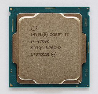
Coffee Lake is Intel's codename for its eighth-generation Core microprocessor family, announced on September 25, 2017. It is manufactured using Intel's second 14 nm process node refinement. Desktop Coffee Lake processors introduced i5 and i7 CPUs featuring six cores and Core i3 CPUs with four cores and no hyperthreading.

<span class="mw-page-title-main">Ryzen</span> AMD brand for microprocessors

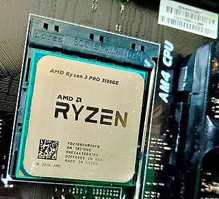
Ryzen is a brand of multi-core x86-64 microprocessors designed and marketed by Advanced Micro Devices (AMD) for desktop, mobile, server, and embedded platforms based on the Zen microarchitecture. It consists of central processing units (CPUs) marketed for mainstream, enthusiast, server, and workstation segments and accelerated processing units (APUs) marketed for mainstream and entry-level segments and embedded systems applications.

<span class="mw-page-title-main">Zen 4</span> 2022 AMD 5-nanometer processor microarchitecture

Zen 4 is the codename for a CPU microarchitecture designed by AMD, released on September 27, 2022. It is the successor to Zen 3 and uses TSMC's N6 process for I/O dies, N5 process for CCDs, and N4 process for APUs. Zen 4 powers Ryzen 7000 performance desktop processors, Ryzen 8000G series mainstream desktop APUs, and Ryzen Threadripper 7000 series HEDT and workstation processors. It is also used in extreme mobile processors, thin & light mobile processors, as well as EPYC 8004/9004 server processors.

<span class="mw-page-title-main">Intel Xe</span> Intel GPU architecture

Intel Xe, earlier known unofficially as Gen12, is a GPU architecture developed by Intel.

Rocket Lake is Intel's codename for its 11th generation Core microprocessors. Released on March 30, 2021, it is based on the new Cypress Cove microarchitecture, a variant of Sunny Cove backported to Intel's 14 nm process node. Rocket Lake cores contain significantly more transistors than Skylake-derived Comet Lake cores.

<span class="mw-page-title-main">Alder Lake</span> Intel microprocessor family

Alder Lake is Intel's codename for the 12th generation of Intel Core processors based on a hybrid architecture utilizing Golden Cove performance cores and Gracemont efficient cores. It is fabricated using Intel's Intel 7 process, previously referred to as Intel 10 nm Enhanced SuperFin (10ESF). The 10ESF has a 10%-15% boost in performance over the 10SF used in the mobile Tiger Lake processors. Intel officially announced 12th Gen Intel Core CPUs on October 27, 2021, mobile CPUs and non-K series desktop CPUs on January 4, 2022, Alder Lake-P and -U series on February 23, 2022, and Alder Lake-HX series on May 10, 2022.

<span class="mw-page-title-main">Apple M1</span> Series of systems-on-a-chip designed by Apple Inc.

Apple M1 is a series of ARM-based system-on-a-chip (SoC) designed by Apple Inc. as a central processing unit (CPU) and graphics processing unit (GPU) for its Mac desktops and notebooks, and the iPad Pro and iPad Air tablets. The M1 chip initiated Apple's third change to the instruction set architecture used by Macintosh computers, switching from Intel to Apple silicon 14 years after they were switched from PowerPC to Intel, and 26 years after the transition from the original Motorola 68000 series to PowerPC. At the time of its introduction in 2020, Apple said that the M1 had the world's fastest CPU core "in low power silicon" and the world's best CPU performance per watt. Its successor, Apple M2, was announced on June 6, 2022, at Worldwide Developers Conference (WWDC).

<span class="mw-page-title-main">Intel Arc</span> Graphics processing unit brand

Intel Arc is a brand of graphics processing units designed by Intel. These are discrete GPUs mostly marketed for the high-margin PC gaming market. The brand also covers Intel's consumer graphics software and services.

Raptor Lake is Intel's codename for the 13th and 14th generations of Intel Core processors based on a hybrid architecture, utilizing Raptor Cove performance cores and Gracemont efficient cores. Like Alder Lake, Raptor Lake is fabricated using Intel's Intel 7 process. Raptor Lake features up to 24 cores and 32 threads and is socket compatible with Alder Lake systems. Like earlier generations, Raptor Lake processors also need accompanying chipsets.

<span class="mw-page-title-main">Apple M2</span> System on a Chip (SoC) designed by Apple Inc.

Apple M2 is a series of ARM-based system on a chip (SoC) designed by Apple Inc. as a central processing unit (CPU) and graphics processing unit (GPU) for its Mac desktops and notebooks, the iPad Pro and iPad Air tablets, and the Vision Pro mixed reality headset. It is the second generation of ARM architecture intended for Apple's Mac computers after switching from Intel Core to Apple silicon, succeeding the M1. Apple announced the M2 on June 6, 2022, at Worldwide Developers Conference (WWDC), along with models of the MacBook Air and the 13-inch MacBook Pro using the M2. The M2 is made with TSMC's "Enhanced 5-nanometer technology" N5P process and contains 20 billion transistors, a 25% increase from the M1. Apple claims CPU improvements up to 18% and GPU improvements up to 35% compared to the M1.

References

  1. "The Intel Innovation 2023 Keynote Live Blog". AnandTech. September 19, 2023. Archived from the original on September 19, 2023. Retrieved September 22, 2023.
  2. "Intel Core Ultra 7 Processor 155H 24M Cache Up To 4.80 GHz Product Specifications". Intel ARK. December 14, 2023. Archived from the original on December 15, 2023. Retrieved December 16, 2023.
  3. 1 2 Schor, David (June 19, 2022). "A Look At Intel 4 Process Technology". WikiChip. Archived from the original on April 12, 2024. Retrieved April 5, 2024. This new node is called Intel 4. For all practical purposes, it is the proper 10-nanometer successor. In other words, had it been released in 2020, it would have properly been called "7nm". Today, it is called 'Intel 4' and is the successor to 'Intel 7' (formerly known as '10nm Enhanced SuperFin', formerly '10nm++').
  4. 1 2 Gomes, Wilfred; Morgan, Slade; Phelps, Boyd; Wilson, Tim; Hallnor, Erik (2022). "Meteor Lake and Arrow Lake Intel Next-Gen 3D Client Architecture Platform with Foveros". 2022 IEEE Hot Chips 34 Symposium (HCS). pp. 1–40. doi:10.1109/HCS55958.2022.9895532. ISBN   978-1-6654-6028-6. S2CID   252551808.
  5. "Intel Core Ultra Ushers in the Age of the AI PC". Intel. Archived from the original on December 14, 2023. Retrieved December 14, 2023.
  6. Intel Corporation, "The 'Blank Sheet' that Delivered Intel's Most Significant SoC Design Change in 40 Years", January, 17, 2004.
  7. 1 2 Liu, Zhiye (July 27, 2021). "Intel Teases 14th-Gen Meteor Lake CPUs With Tile Design and 192 EUs". Tom's Hardware. Archived from the original on April 5, 2024. Retrieved April 5, 2024.
  8. "Intel's 7nm "Meteor Lake" compute tile has taped in". VideoCardz. May 24, 2021. Archived from the original on April 5, 2024. Retrieved April 5, 2024.
  9. Shilov, Anton (October 22, 2021). "Intel: 14th Gen Meteor Lake Compute Tile Powers On, Performs Well". Tom's Hardware. Archived from the original on April 5, 2024. Retrieved April 5, 2024.
  10. "14th Gen Core "Meteor Lake" has been powered-on, on track to launch in 2023". VideoCardz. April 29, 2022. Archived from the original on April 5, 2024. Retrieved April 5, 2024.
  11. Mujtaba, Hassan (April 29, 2022). "Intel Achieves 14th Gen Meteor Lake CPU 'Power-On' With Launch Scheduled For 2023". Wccftech. Archived from the original on April 5, 2024. Retrieved April 5, 2024.
  12. Norem, Josh (March 17, 2023). "Rumor: Intel to Cancel Meteor Lake Desktop, Replace It With Arrow Lake". ExtremeTech. Archived from the original on April 5, 2024. Retrieved April 5, 2024.
  13. "Intel's 2024 Arrow Lake-S desktop CPUs to feature up to 24 cores and support DDR5-6400 memory". VideoCardz. March 17, 2023. Archived from the original on April 5, 2024. Retrieved April 5, 2024.
  14. Bonshor, Gavin (September 26, 2023). "Intel Meteor Lake SoC is NOT Coming to Desktops: Well, Not Technically". AnandTech. Archived from the original on December 8, 2023. Retrieved April 5, 2024.
  15. Laird, Jeremy (September 26, 2023). "Once, finally and for all Intel's Meteor Lake is not coming to the desktop CPU sockets". PC Gamer. Archived from the original on April 5, 2024. Retrieved April 5, 2024.
  16. Shilov, Anton (September 26, 2023). "Intel Clarifies Meteor Lake is Not for Desktop PCs: Not in Socketed Form". Tom's Hardware. Archived from the original on April 5, 2024. Retrieved April 5, 2024.
  17. Rißka, Volker (September 26, 2023). "For notebooks & AIOs: Intel Meteor Lake is not available for "classic desktop PCs"". ComputerBase (in German). Archived from the original on January 7, 2024. Retrieved April 5, 2024.
  18. Robinson, Cliff (June 15, 2023). "Intel Overhauls Core Branding with Meteor Lake". ServeTheHome. Archived from the original on April 5, 2024. Retrieved April 5, 2024.
  19. Bonshor, Gavin (June 15, 2023). "Intel To Launch New Core Processor Branding for Meteor Lake: Drop the i, Add Ultra Tier". AnandTech. Archived from the original on April 5, 2024. Retrieved April 5, 2024.
  20. Thubron, Rob (June 15, 2023). "Intel announces biggest processor rebranding in 15 years ahead of Meteor Lake launch". TechSpot. Archived from the original on April 5, 2024. Retrieved April 5, 2024.
  21. Sandhu, Tarinder (June 15, 2023). "Intel's radical simplification of Core branding only adds to the confusion". Club386. Archived from the original on April 5, 2024. Retrieved April 5, 2024.
  22. Loeffler, John (June 15, 2023). "Intel's new processor branding drops the 'i' – and the ball". TechRadar. Archived from the original on April 5, 2024. Retrieved April 5, 2024.
  23. White, Monica J. (June 15, 2023). "Intel just admitted defeat". Digital Trends. Archived from the original on April 5, 2024. Retrieved April 5, 2024.
  24. Smith, Ryan (April 27, 2023). "Intel: Meteor Lake & Intel 4 Process Now Ramping for Production". AnandTech. Archived from the original on April 5, 2024. Retrieved April 5, 2024.
  25. Zuhair, Muhammad (August 24, 2023). "Intel Expresses Confidence in "Intel 4" Process, Says Its Competitive With TSMC's 3nm Node". Wccftech. Archived from the original on April 5, 2024. Retrieved April 5, 2024.
  26. Zuhair, Muhammad (August 28, 2023). "Intel Could Dish Out An Estimated 365,000 Next-Gen Meteor Lake CPU Tiles Per Month". Wccftech. Archived from the original on April 5, 2024. Retrieved April 5, 2024.
  27. Norem, Josh (August 28, 2023). "Intel Projected to Pump Out 365,000 Meteor Lake CPUs a Month". ExtremeTech. Archived from the original on April 5, 2024. Retrieved April 5, 2024.
  28. "Fab 34 reaches important Intel 4 milestone". Intel in Ireland. August 22, 2023. Archived from the original on April 5, 2024. Retrieved April 5, 2024.
  29. "Intel's New Fab in Ireland Begins High-Volume Production of Intel 4 Technology". Intel Newsroom (Press release). Leixlip, Ireland. September 29, 2023. Archived from the original on April 5, 2024. Retrieved April 5, 2024.
  30. Hardawar, Devindra (September 19, 2023). "Intel's Core Ultra 'Meteor Lake' chips arrive on December 14". Engadget. Archived from the original on April 5, 2024. Retrieved April 5, 2024.
  31. 1 2 Khullar, Kunal (September 19, 2023). "Intel's Core Ultra CPUs are more Apple, less AMD". Digital Trends. Archived from the original on April 5, 2024. Retrieved April 5, 2024.
  32. Lilly, Paul (July 13, 2017). "Intel slide criticizes AMD for using "glued-together" dies in Epyc processors". PC Gamer. Retrieved May 23, 2024.
  33. Westover, Brian (September 19, 2023). "'Meteor Lake' Architecture Detailed: What to Know About Intel's Next-Gen CPUs". PCMag. Retrieved May 23, 2024.
  34. Temsamani, Fahd (August 24, 2022). "Intel reveals key details about 3D Foveros chip design on Meteor Lake". Club386.
  35. Deutscher, Maria (July 25, 2022). "Intel to produce chips for MediaTek as part of new partnership". Silicon Angle. Retrieved May 23, 2024.
  36. Mehta, Rich (February 5, 2019). "Intel announces tweaks to 22FFL process for RF, MRAM at IEDM18". Semiconductor Digest. Retrieved May 23, 2024.
  37. Alcorn, Paul (April 27, 2023). "Intel's Meteor Lake, Its First PC Chips With TSMC Tech, Launch This Year". Tom's Hardware. Retrieved May 23, 2024.
  38. Alcorn, Paul (September 19, 2023). "Intel Details Core Ultra 'Meteor Lake' Architecture, Launches December 14". Tom's Hardware. Retrieved May 23, 2024.
  39. 1 2 3 4 Zuhair, Muhammad (August 28, 2023). "Intel Could Dish Out An Estimated 365,000 Next-Gen Meteor Lake CPU Tiles Per Month". Wccftech. Retrieved May 23, 2024.
  40. "Meteor Lake's E-Cores: Crestmont Makes Incremental Progress". Chips and Cheese. May 13, 2024. Retrieved May 23, 2024.
  41. 1 2 3 4 Alcorn, Paul (September 19, 2023). "Intel Details Core Ultra 'Meteor Lake' Architecture, Launches December 14". Tom's Hardware. Retrieved May 23, 2024.
  42. Connatser, Matthew (January 2, 2024). "Intel's Meteor Lake CPUs are slower at single-core work than previous-gen models — new benchmarks show IPC regressions vs Raptor Lake". Tom's Hardware. Retrieved May 23, 2024.
  43. Bonshor, Gavin (September 19, 2023). "Compute Tile: New P (Redwood Cove) and E-cores (Crestmont)". AnandTech. Retrieved May 23, 2024.
  44. 1 2 Walton, Jarred (September 19, 2023). "Intel's Meteor Lake GPU Doubles Integrated Graphics Performance Per Watt". Tom's Hardware. Retrieved May 23, 2024.
  45. "Intel's Ambitious Meteor Lake iGPU". Chips and Cheese. April 8, 2024. Retrieved May 23, 2024.
  46. Cunningham, Andrew (September 20, 2023). "Intel's biggest laptop CPU update in years is a huge departure from past designs". Ars Technica. Retrieved May 23, 2024.
  47. Hollister, Sean (September 19, 2023). "Intel will launch Meteor Lake on December 14th — this is Intel's Core Ultra". The Verge. Retrieved May 23, 2024.
  48. Ridley, Jacob (September 19, 2023). "I didn't need a graphics card to play Dying Light 2 on Intel's new laptop chip". PC Gamer. Retrieved May 23, 2024.
  49. "Dell confirms Intel Core Ultra 155H/125H specs, Arc iGPU requires dual-channel 16GB memory". VideoCardz. November 22, 2023. Retrieved May 23, 2024.
  50. Hachman, Mark (September 19, 2023). "6 ways Intel's new 14th-gen 'Meteor Lake' CPUs supercharge laptops". PCWorld. Retrieved May 23, 2024.
  51. 1 2 Bonshor, Gavin (September 19, 2023). "Intel Unveils Meteor Lake Architecture: Intel 4 Heralds the Disaggregated Future of Mobile CPUs". AnandTech. Retrieved May 23, 2024.
  52. Liu, Zhiye (May 20, 2023). "Intel Meteor Lake 16-Core, 14-Core CPUs Surface In New Benchmarks". Tom's Hardware. Retrieved May 23, 2024.
  53. 1 2 Shankland, Stephen; Grunin, Lori (September 19, 2023). "Intel Tucks Battery-Saving Tricks Into Its Meteor Lake PC Processor". CNET. Retrieved May 23, 2024.
  54. "Comparing Crestmonts: No L3 Hurts". Chips and Cheese. May 20, 2024. Retrieved May 23, 2024.
  55. Wilson, Jason R. (December 28, 2022). "Intel Meteor Lake Confirmed To Offer AV1 Encoding & Decoding Support". Wccftech. Retrieved May 23, 2024.
  56. Norem, Josh (May 24, 2023). "Intel Announces an Integrated Neural AI Accelerator in Meteor Lake". ExtremeTech. Retrieved May 23, 2024.
  57. Smith, Ryan (May 29, 2023). "Intel Discloses New Details On Meteor Lake VPU Block, Lays Out Vision For Client AI". AnandTech. Retrieved May 23, 2024.
  58. 1 2 "Intel Meteor Lake's NPU". Chips and Cheese. April 22, 2024. Retrieved May 23, 2024.
  59. Laird, Jeremy (May 30, 2023). "Intel demos Stable Diffusion running locally on its new AI-accelerated Meteor Lake CPU". PC Gamer. Retrieved May 23, 2024.
  60. 1 2 Kan, Michael (September 19, 2023). "The 'Meteor Lake' NPU: Meet Intel's Dedicated Silicon for Local AI Processing". PCMag.
  61. Hachman, Mark (July 28, 2023). "Meteor Lake CPUs will launch the 'AI PC' era, Intel CEO proclaims". PCWorld. Retrieved May 23, 2024.
  62. Bonshor, Gavin (September 19, 2023). "I/O Tile: Extended and Scalable Depending on Segment". AnandTech. Retrieved May 23, 2024.
  63. Kennedy, Patrick (August 26, 2022). "Intel Enters a New Era of Chiplets that will Change Everything". ServeTheHome. Retrieved May 23, 2024.
  64. Hachman, Mark (June 10, 2020). "Intel announces its first new 'Lakefield' chips for the thinnest, lightest PCs". PCWorld. Retrieved May 23, 2024.
  65. Cutress, Ian (July 2, 2020). "The Intel Lakefield Deep Dive: Everything To Know About the First x86 Hybrid CPU". AnandTech. Retrieved May 23, 2024.
  66. Hruska, Joel (July 8, 2021). "Intel Discontinues Lakefield, Its First x86 Hybrid CPU". ExtremeTech. Retrieved May 23, 2024.