Intel Core (microarchitecture)

Last updated

Intel Core
General information
LaunchedJune 26, 2006;17 years ago (June 26, 2006) (Xeon)
July 27, 2006;17 years ago (July 27, 2006) (Core 2)
Performance
Max. CPU clock rate 933 MHz to 3.5 GHz
FSB speeds533  MT/s to 1600 MT/s
Cache
L1 cache 64 KB per core
L2 cache0.5 to 6 MB per two cores
L3 cache8 MB to 16 MB shared (Xeon 7400)
Architecture and classification
Technology node 65 nm to 45 nm
Microarchitecture Core
Instruction set x86-16, IA-32, x86-64
Extensions
Physical specifications
Transistors
Cores
  • 1–4 (2-6 Xeon)
Socket(s)
Products, models, variants
Model(s)
History
Predecessor(s) NetBurst
Enhanced Pentium M (P6)
Successor(s) Penryn (tick)
(a version of Core)
Nehalem (tock)
Support status
Unsupported

The Intel Core microarchitecture (provisionally referred to as Next Generation Micro-architecture, [1] and developed as Merom) [2] is a multi-core processor microarchitecture launched by Intel in mid-2006. It is a major evolution over the Yonah, the previous iteration of the P6 microarchitecture series which started in 1995 with Pentium Pro. It also replaced the NetBurst microarchitecture, which suffered from high power consumption and heat intensity due to an inefficient pipeline designed for high clock rate. In early 2004 the new version of NetBurst (Prescott) needed very high power to reach the clocks it needed for competitive performance, making it unsuitable for the shift to dual/multi-core CPUs. On May 7, 2004 Intel confirmed the cancellation of the next NetBurst, Tejas and Jayhawk. [3] Intel had been developing Merom, the 64-bit evolution of the Pentium M, since 2001, [2] and decided to expand it to all market segments, replacing NetBurst in desktop computers and servers. It inherited from Pentium M the choice of a short and efficient pipeline, delivering superior performance despite not reaching the high clocks of NetBurst. [lower-alpha 1]

Contents

The first processors that used this architecture were code-named 'Merom', 'Conroe', and 'Woodcrest'; Merom is for mobile computing, Conroe is for desktop systems, and Woodcrest is for servers and workstations. While architecturally identical, the three processor lines differ in the socket used, bus speed, and power consumption. The first Core-based desktop and mobile processors were branded Core 2 , later expanding to the lower-end Pentium Dual-Core , Pentium and Celeron brands; while server and workstation Core-based processors were branded Xeon .

Features

The Core microarchitecture returned to lower clock rates and improved the use of both available clock cycles and power when compared with the preceding NetBurst microarchitecture of the Pentium 4 and D-branded CPUs. [4] The Core microarchitecture provides more efficient decoding stages, execution units, caches, and buses, reducing the power consumption of Core 2-branded CPUs while increasing their processing capacity. Intel's CPUs have varied widely in power consumption according to clock rate, architecture, and semiconductor process, shown in the CPU power dissipation tables.

Like the last NetBurst CPUs, Core based processors feature multiple cores and hardware virtualization support (marketed as Intel VT-x), and Intel 64 and SSSE3. However, Core-based processors do not have the hyper-threading technology as in Pentium 4 processors. This is because the Core microarchitecture is based on the P6 microarchitecture used by Pentium Pro, II, III, and M.

The L1 cache of the Core microarchitecture at 64 KB L1 cache/core (32 KB L1 Data + 32 KB L1 Instruction) is as large as in Pentium M, up from 32 KB on Pentium II / III (16 KB L1 Data + 16 KB L1 Instruction). The consumer version also lacks an L3 cache as in the Gallatin core of the Pentium 4 Extreme Edition, though it is exclusively present in high-end versions of Core-based Xeons. Both an L3 cache and hyper-threading were reintroduced again to consumer line in the Nehalem microarchitecture.

Roadmap

Technology

Intel Core microarchitecture Intel Core2 arch.svg
Intel Core microarchitecture

While the Core microarchitecture is a major architectural revision, it is based in part on the Pentium M processor family designed by Intel Israel. [5] The pipeline of Core/Penryn is 14 stages long [6] – less than half of Prescott's. Penryn's successor Nehalem has a two cycles higher branch misprediction penalty than Core/Penryn. [7] [8] Core can ideally sustain up to 4 instructions per cycle (IPC) execution rate, compared to the 3 IPC capability of P6, Pentium M and NetBurst microarchitectures. The new architecture is a dual core design with a shared L2 cache engineered for maximum performance per watt and improved scalability.

One new technology included in the design is Macro-Ops Fusion, which combines two x86 instructions into a single micro-operation. For example, a common code sequence like a compare followed by a conditional jump would become a single micro-op. However, this technology does not work in 64-bit mode.

Core can speculatively execute loads ahead of preceding stores with unknown addresses. [9]

Other new technologies include 1 cycle throughput (2 cycles previously) of all 128-bit SSE instructions and a new power saving design. All components will run at minimum speed, raising speed dynamically as needed (similar to AMD's Cool'n'Quiet power-saving technology, and Intel's own SpeedStep technology from earlier mobile processors). This allows the chip to produce less heat, and minimize power use.

For most Woodcrest CPUs, the front-side bus (FSB) runs at 1333 MT/s; however, this is scaled down to 1066 MT/s for lower end 1.60 and 1.86 GHz variants. [10] [11] The Merom mobile variant was initially targeted to run at an FSB of 667 MT/s while the second wave of Meroms, supporting 800 MT/s FSB, were released as part of the Santa Rosa platform with a different socket in May 2007. The desktop-oriented Conroe began with models having an FSB of 800 MT/s or 1066 MT/s with a 1333 MT/s line officially launched on July 22, 2007.

The power use of these processors is very low: average energy use is to be in the 1–2 watt range in ultra low voltage variants, with thermal design powers (TDPs) of 65 watts for Conroe and most Woodcrests, 80 watts for the 3.0 GHz Woodcrest, and 40 or 35 watts for the low-voltage Woodcrest. In comparison, a 2.2 GHz AMD Opteron 875HE processor consumes 55 watts, while the energy efficient Socket AM2 line fits in the 35 watt thermal envelope (specified a different way so not directly comparable). Merom, the mobile variant, is listed at 35 watts TDP for standard versions and 5 watts TDP for ultra low voltage (ULV) versions.[ citation needed ]

Previously, Intel announced that it would now focus on power efficiency, rather than raw performance. However, at Intel Developer Forum (IDF) in spring 2006, Intel advertised both. Some of the promised numbers were:

Processor cores

The processors of the Core microarchitecture can be categorized by number of cores, cache size, and socket; each combination of these has a unique code name and product code that is used across several brands. For instance, code name "Allendale" with product code 80557 has two cores, 2 MB L2 cache and uses the desktop socket 775, but has been marketed as Celeron, Pentium, Core 2, and Xeon, each with different sets of features enabled. Most of the mobile and desktop processors come in two variants that differ in the size of the L2 cache, but the specific amount of L2 cache in a product can also be reduced by disabling parts at production time. Tigerton dual-cores and all quad-core processors except - are multi-chip modules combining two dies. For the 65 nm processors, the same product code can be shared by processors with different dies, but the specific information about which one is used can be derived from the stepping.

CoresMobileDesktop, UP ServerCL ServerDP ServerMP Server
Single-Core 65 nm 1 Merom-L
80537
Conroe-L
80557
Single-Core 45 nm Penryn-L
80585
Wolfdale-CL
80588
Dual-Core 65 nm2 Merom-2M
80537
Merom
80537
Allendale
80557
Conroe
80557
Conroe-CL
80556
Woodcrest
80556
Tigerton
80564
Dual-Core 45 nm Penryn-3M
80577
Penryn
80576
Wolfdale-3M
80571
Wolfdale
80570
Wolfdale-CL
80588
Wolfdale-DP
80573
Quad-Core 65 nm4 Kentsfield
80562
Clovertown
80563
Tigerton QC
80565
Quad-Core 45 nm Penryn-QC
80581
Yorkfield-6M
80580
Yorkfield
80569
Yorkfield-CL
80584
Harpertown
80574
Dunnington QC
80583
Six-Core 45 nm6 Dunnington
80582

Conroe/Merom (65 nm)

The original Core 2 processors are based on the same dies that can be identified as CPUID Family 6 Model 15. Depending on their configuration and packaging, their code names are Conroe (LGA 775, 4 MB L2 cache), Allendale (LGA 775, 2 MB L2 cache), Merom (Socket M, 4 MB L2 cache) and Kentsfield (multi-chip module, LGA 775, 2x4MB L2 cache). Merom and Allendale processors with limited features are in Pentium Dual Core and Celeron processors, while Conroe, Allendale and Kentsfield also are sold as Xeon processors.

Additional code names for processors based on this model are Woodcrest (LGA 771, 4 MB L2 cache), Clovertown (MCM, LGA 771, 2×4MB L2 cache) and Tigerton (MCM, Socket 604, 2×4MB L2 cache), all of which are marketed only under the Xeon brand.

ProcessorBrand nameModel (list)CoresL2 CacheSocketTDP
Mobile processors
Merom-2MMobile Core 2 Duo U7xxx 22 MBBGA47910 W
Merom L7xxx 4 MB17 W
Merom
Merom-2M
T5xxx
T7xxx
2–4 MB Socket M
Socket P
BGA479
35 W
Merom XEMobile Core 2 Extreme X7xxx 24 MBSocket P44 W
Merom Celeron M 5x0 11 MBSocket M
Socket P
30 W
Merom-2M 5x5 Socket P31 W
Merom-2MCeleron Dual-Core T1xxx 2512–1024 KB35 W
Merom-2M Pentium Dual-Core T2xxx
T3xxx
21 MB35 W
Desktop processors
Allendale Xeon 3xxx 22 MB LGA 775 65 W
Conroe 3xxx 2–4 MB
Conroe and
Allendale
Core 2 Duo E4xxx 22 MBLGA 77565 W
E6xx0 2–4 MB
Conroe-CL E6xx5 2–4 MB LGA 771
Conroe-XE Core 2 Extreme X6xxx 24 MBLGA 77575 W
Allendale Pentium Dual-Core E2xxx 21 MB65 W
Allendale Celeron E1xxx 2512 KB65 W
Kentsfield Xeon 32xx 42×4 MB95–105 W
Kentsfield Core 2 Quad Q6xxx 42×4 MB95–105 W
Kentsfield XE Core 2 Extreme QX6xxx 42×4 MB130 W
Woodcrest Xeon 51xx 24 MBLGA 77165–80 W
Clovertown L53xx 42×4 MBLGA 77140–50 W
E53xx80 W
X53xx120–150 W
Tigerton E72xx 22×4 MB Socket 604 80 W
Tigerton QC L73xx450 W
E73xx2×2–2×4 MB80 W
X73xx2×4 MB130 W

Conroe-L/Merom-L

The Conroe-L and Merom-L processors are based around the same core as Conroe and Merom, but only contain a single core and 1 MB of L2 cache, significantly reducing production cost and power consumption of the processor at the expense of performance compared to the dual-core version. It is used only in ultra-low voltage Core 2 Solo U2xxx and in Celeron processors and is identified as CPUID family 6 model 22.

ProcessorBrand nameModel (list)CoresL2 CacheSocketTDP
Merom-LMobile Core 2 Solo U2xxx 12 MBBGA4795.5 W
Merom-L Celeron M 5x0 1512 KBSocket M
Socket P
27 W
Merom-L 5x3 512–1024 KBBGA4795.5–10 W
Conroe-L Celeron M 4x0 1512 KBLGA 77535 W
Conroe-CL 4x5 LGA 77165 W

Penryn/Wolfdale (45 nm)

Wolfdale-type Core 2 Duo E8400 top view Intel CPU Core 2 Duo E8400 Wolfdale top.jpg
Wolfdale-type Core 2 Duo E8400 top view
Wolfdale-type Core 2 Duo E8400 perspective view Intel CPU Core 2 Duo E8400 Wolfdale perspective.jpg
Wolfdale-type Core 2 Duo E8400 perspective view

In Intel's Tick-Tock cycle, the 2007/2008 "Tick" was the shrink of the Core microarchitecture to 45 nanometers as CPUID model 23. In Core 2 processors, it is used with the code names Penryn (Socket P), Wolfdale (LGA 775) and Yorkfield (MCM, LGA 775), some of which are also sold as Celeron, Pentium and Xeon processors. In the Xeon brand, the Wolfdale-DP and Harpertown code names are used for LGA 771 based MCMs with two or four active Wolfdale cores.

Architecturally, 45 nm Core 2 processors feature SSE4.1 and new divide/shuffle engine. [12]

The chips come in two sizes, with 6 MB and 3 MB L2 cache. The smaller version is commonly called Penryn-3M and Wolfdale-3M and Yorkfield-6M, respectively. The single-core version of Penryn, listed as Penryn-L here, is not a separate model like Merom-L but a version of the Penryn-3M model with only one active core.

ProcessorBrand nameModel (list)CoresL2 CacheSocketTDP
Mobile processors
Penryn-L Core 2 Solo SU3xxx 13 MBBGA9565.5 W
Penryn-3M Core 2 Duo SU7xxx 23 MBBGA95610 W
SU9xxx
Penryn SL9xxx 6 MB17 W
SP9xxx 25/28 W
Penryn-3M P7xxx 3 MB Socket P
FCBGA6
25 W
P8xxx
Penryn P9xxx 6 MB
Penryn-3M T6xxx 2 MB35 W
T8xxx 3 MB
Penryn T9xxx 6 MB
E8x35 6 MBSocket P35-55 W
Penryn-QCCore 2 Quad Q9xxx 42x3-2x6 MBSocket P45 W
Penryn XECore 2 Extreme X9xxx 26 MBSocket P44 W
Penryn-QC QX9300 42x6 MB45 W
Penryn-3M Celeron T3xxx 21 MBSocket P35 W
SU2xxx µFC-BGA 95610 W
Penryn-L 9x0 11 MBSocket P35 W
7x3 µFC-BGA 95610 W
Penryn-3M Pentium T4xxx 21 MBSocket P35 W
SU4xxx 2 MBµFC-BGA 95610 W
Penryn-L SU2xxx 15.5 W
Desktop processors
Wolfdale-3M Celeron E3xxx 21 MBLGA 77565 W
Pentium E2210
E5xxx 2 MB
E6xxx
Core 2 Duo E7xxx 3 MB
Wolfdale E8xxx 6 MB
Xeon 31x0 45-65 W
Wolfdale-CL 30x4 1 LGA 771 30 W
31x3 265 W
Yorkfield X33x0 42×3–2×6 MB LGA 775 65–95 W
Yorkfield-CL X33x3 LGA 771 80 W
Yorkfield-6M Core 2 Quad Q8xxx 2×2 MBLGA 77565–95 W
Q9x0x 2×3 MB
Yorkfield Q9x5x 2×6 MB
Yorkfield XECore 2 Extreme QX9xxx 2×6 MB130–136 W
QX9xx5 LGA 771150 W
Wolfdale-DP Xeon E52xx 26 MB65 W
L52xx20-55 W
X52xx80 W
Harpertown E54xx 42×6 MBLGA 771
L54xx40-50 W
X54xx120-150 W

Dunnington

The Xeon "Dunnington" processor (CPUID Family 6, model 29) is closely related to Wolfdale but comes with six cores and an on-chip L3 cache and is designed for servers with Socket 604, so it is marketed only as Xeon, not as Core 2.

ProcessorBrand nameModel (list)CoresL3 cacheSocketTDP
Dunnington Xeon E74xx 4-68-16 MB Socket 604 90 W
L74xx4-612 MB50-65 W
X7460616 MB130 W

Steppings

The Core microarchitecture uses several stepping levels (steppings), which unlike prior microarchitectures, represent incremental improvements, and different sets of features like cache size and low power modes. Most of these steppings are used across brands, typically by disabling some features and limiting clock frequencies on low-end chips.

Steppings with a reduced cache size use a separate naming scheme, which means that the releases are no longer in alphabetic order. Added steppings have been used in internal and engineering samples, but are unlisted in the tables.

Many of the high-end Core 2 and Xeon processors use Multi-chip modules of two chips in order to get larger cache sizes or more than two cores.

Steppings using 65 nm process

Mobile (Merom)Desktop (Conroe)Desktop (Kentsfield)Server (Woodcrest, Clovertown, Tigerton)
SteppingReleasedAreaCPUIDL2 cacheMax. clockCeleronPentiumCore 2CeleronPentiumCore 2XeonCore 2XeonXeon
B2Jul 2006143 mm²06F64 MB2.93 GHz M5xx T5000 T7000 L7000 E6000 X6000 3000 5100
B3Nov 2006143 mm²06F74 MB3.00 GHz Q6000 QX6000 3200 5300
L2Jan 2007111 mm²06F22 MB2.13 GHz T5000 U7000 E2000 E4000 E6000 3000
E1May 2007143 mm²06FA4 MB2.80 GHz M5xx T7000 L7000 X7000
G0Apr 2007143 mm²06FB4 MB3.00 GHz M5xx T7000 L7000 X7000 E2000 E4000 E6000 3000 Q6000 QX6000 3200 5100 5300 7200 7300
G2Mar 2009 [13] 143 mm²06FB4 MB2.16 GHz M5xx T5000 T7000 L7000
M0Jul 2007111 mm²06FD2 MB2.40 GHz 5xx T1000 T2000 T3000 T5000 T7000 U7000 E1000 E2000 E4000
A1Jun 200781 mm² [lower-alpha 2] 106611 MB2.20 GHz M5xx U2000 220 4x0

Early ES/QS steppings are: B0 (CPUID 6F4h), B1 (6F5h) and E0 (6F9h).

Steppings B2/B3, E1, and G0 of model 15 (cpuid 06fx) processors are evolutionary steps of the standard Merom/Conroe die with 4 MB L2 cache, with the short-lived E1 stepping only being used in mobile processors. Stepping L2 and M0 are the Allendale chips with just 2 MB L2 cache, reducing production cost and power consumption for low-end processors.

The G0 and M0 steppings improve idle power consumption in C1E state and add the C2E state in desktop processors. In mobile processors, all of which support C1 through C4 idle states, steppings E1, G0, and M0 add support for the Mobile Intel 965 Express (Santa Rosa) platform with Socket P, while the earlier B2 and L2 steppings only appear for the Socket M based Mobile Intel 945 Express (Napa refresh) platform.

The model 22 stepping A1 (cpuid 10661h) marks a significant design change, with just a single core and 1 MB L2 cache further reducing the power consumption and manufacturing cost for the low-end. Like the earlier steppings, A1 is not used with the Mobile Intel 965 Express platform.

Steppings G0, M0 and A1 mostly replaced all older steppings in 2008. In 2009, a new stepping G2 was introduced to replace the original stepping B2. [16]

Steppings using 45 nm process

Mobile (Penryn)Desktop (Wolfdale)Desktop (Yorkfield)Server (Wolfdale-DP, Harpertown, Dunnington)
SteppingReleasedAreaCPUIDL2 cacheMax. clock Celeron Pentium Core 2 Celeron Pentium Core 2 Xeon Core 2 Xeon Xeon
C0Nov 2007107 mm²106766 MB3.00 GHz E8000 P7000 T8000 T9000 P9000 SP9000 SL9000 X9000 E8000 3100 QX9000 5200 5400
M0Mar 200882 mm²106763 MB2.40 GHz 7xx SU3000 P7000 P8000 T8000 SU9000 E5000 E2000 E7000
C1Mar 2008107 mm²106776 MB3.20 GHz Q9000 QX9000 3300
M1Mar 200882 mm²106773 MB2.50 GHz Q8000 Q9000 3300
E0Aug 2008107 mm²1067A6 MB3.33 GHz T9000 P9000 SP9000 SL9000 Q9000 QX9000 E8000 3100 Q9000 Q9000S QX9000 3300 5200 5400
R0Aug 200882 mm²1067A3 MB2.93 GHz 7xx 900 SU2000 T3000 T4000 SU2000 SU4000 SU3000 T6000 SU7000 P8000 SU9000 E3000 E5000 E6000 E7000 Q8000 Q8000S Q9000 Q9000S 3300
A1Sep 2008503 mm²106D13 MB2.67 GHz 7400

In the model 23 (cpuid 01067xh), Intel started marketing stepping with full (6 MB) and reduced (3 MB) L2 cache at the same time, and giving them identical cpuid values. All steppings have the new SSE4.1 instructions. Stepping C1/M1 was a bug fix version of C0/M0 specifically for quad core processors and only used in those. Stepping E0/R0 adds two new instructions (XSAVE/XRSTOR) and replaces all earlier steppings.

In mobile processors, stepping C0/M0 is only used in the Intel Mobile 965 Express (Santa Rosa refresh) platform, whereas stepping E0/R0 supports the later Intel Mobile 4 Express (Montevina) platform.

Model 30 stepping A1 (cpuid 106d1h) adds an L3 cache and six instead of the usual two cores, which leads to an unusually large die size of 503 mm². [17] As of February 2008, it has only found its way into the very high-end Xeon 7400 series (Dunnington).

System requirements

Motherboard compatibility

Conroe, Conroe XE and Allendale all use Socket LGA 775; however, not every motherboard is compatible with these processors.

Supporting chipsets are:

The Yorkfield XE model QX9770 (45 nm with 1600 MT/s FSB) has limited chipset compatibility - with only X38, P35 (With Overclocking) and some high-performance X48 and P45 motherboards being compatible. BIOS updates were gradually being released to provide support for the Penryn technology, and the QX9775 is only compatible with the Intel D5400XS motherboard. The Wolfdale-3M model E7200 also has limited compatibility (at least the Xpress 200 chipset is incompatible)[ citation needed ].

Although a motherboard may have the required chipset to support Conroe, some motherboards based on the above-mentioned chipsets do not support Conroe. This is because all Conroe-based processors require a new power delivery feature set specified in Voltage Regulator-Down (VRD) 11.0. This requirement is a result of Conroe's significantly lower power consumption, compared to the Pentium 4/D CPUs it replaced. A motherboard that has both a supporting chipset and VRD 11 supports Conroe processors, but even then some boards will need an updated BIOS to recognize Conroe's FID (Frequency ID) and VID (Voltage ID).

Synchronous memory modules

Unlike the prior Pentium 4 and Pentium D design, the Core 2 technology sees a greater benefit from memory running synchronously with the front-side bus (FSB). This means that for the Conroe CPUs with FSB of 1066 MT/s, the ideal memory performance for DDR2 is PC2-8500. In a few configurations, using PC2-5300 instead of PC2-4200 can actually decrease performance. Only when going to PC2-6400 is there a significant performance increase. While DDR2 memory models with tighter timing specifications do improve performance, the difference in real world games and applications is often negligible. [18]

Optimally, the memory bandwidth afforded should match the bandwidth of the FSB, that is to say that a CPU with a 533 MT/s rated bus speed should be paired with RAM matching the same rated speed, for example DDR2 533, or PC2-4200. A common myth[ citation needed ] is that installing interleaved RAM will offer double the bandwidth. However, at most the increase in bandwidth by installing interleaved RAM is roughly 5–10%. The AGTL+ PSB used by all NetBurst processors and current and medium-term (pre-QuickPath) Core 2 processors provide a 64-bit data path. Current chipsets provide for a couple of either DDR2 or DDR3 channels.

Matched processor and RAM ratings
Processor modelFront-side busMatched memory and maximum bandwidth
single channel, dual channel
DDR DDR2 DDR3
Mobile: T5200, T5300, U2n00, U7n00533 MT/s PC-3200 (DDR-400)
3.2 GB/s
PC2-4200 (DDR2-533)
4.264 GB/s
PC2-8500 (DDR2-1066)
8.532 GB/s
PC3-8500 (DDR3-1066)
8.530 GB/s
Desktop: E6n00, E6n20, X6n00, E7n00, Q6n00 and QX6n00
Mobile: T9400, T9550, T9600, P7350, P7450, P8400, P8600, P8700, P9500, P9600, SP9300, SP9400, X9100
1066 MT/s
Mobile: T5n00, T5n50, T7n00 (Socket M), L7200, L7400667 MT/sPC-3200 (DDR-400)
3.2 GB/s
PC2-5300 (DDR2-667)
5.336 GB/s
PC3-10600 (DDR3-1333)
10.670 GB/s
Desktop: E6n40, E6n50, E8nn0, Q9nn0, QX6n50, QX96501333 MT/s
Mobile: T5n70, T6400, T7n00 (Socket P), L7300, L7500, X7n00, T8n00, T9300, T9500, X9000
Desktop: E4n00, Pentium E2nn0, Pentium E5nn0, Celeron 4n0, E3n00
800 MT/sPC-3200 (DDR-400)
3.2 GB/s
PC-3200 (DDR-400)
3.2 GB/s
PC2-6400 (DDR2-800)
6.400 GB/s
PC2-8500 (DDR2-1066)
8.532 GB/s
PC3-6400 (DDR3-800)
6.400 GB/s
PC3-12800 (DDR3-1600)
12.800 GB/s
Desktop: QX9770, QX97751600 MT/s

On jobs requiring large amounts of memory access, the quad-core Core 2 processors can benefit significantly [19] from using PC2-8500 memory, which runs at the same speed as the CPU's FSB; this is not an officially supported configuration, but several motherboards support it.

The Core 2 processor does not require the use of DDR2. While the Intel 975X and P965 chipsets require this memory, some motherboards and chipsets support both Core 2 processors and DDR memory. When using DDR memory, performance may be reduced because of the lower available memory bandwidth.

Chip errata

The Core 2 memory management unit (MMU) in X6800, E6000 and E4000 processors does not operate to prior specifications implemented in prior generations of x86 hardware. This may cause problems, many of them serious security and stability issues, with extant operating system software. Intel's documentation states that their programming manuals will be updated "in the coming months" with information on recommended methods of managing the translation lookaside buffer (TLB) for Core 2 to avoid issues, and admits that, "in rare instances, improper TLB invalidation may result in unpredictable system behavior, such as hangs or incorrect data." [20]

Among the issues stated:

Intel errata Ax39, Ax43, Ax65, Ax79, Ax90, Ax99 are said to be particularly serious. [21] 39, 43, 79, which can cause unpredictable behavior or system hang, have been fixed in recent steppings.

Among those who have stated the errata to be particularly serious are OpenBSD's Theo de Raadt [22] and DragonFly BSD's Matthew Dillon. [23] Taking a contrasting view was Linus Torvalds, calling the TLB issue "totally insignificant", adding, "The biggest problem is that Intel should just have documented the TLB behavior better." [24]

Microsoft has issued update KB936357 to address the errata by microcode update, [25] with no performance penalty. BIOS updates are also available to fix the issue.

See also

Related Research Articles

<span class="mw-page-title-main">Celeron</span> Line of discontinued microprocessors made by Intel

Celeron is a discontinued series of low-end IA-32 and x86-64 computer microprocessor models targeted at low-cost personal computers, manufactured by Intel. The first Celeron-branded CPU was introduced on April 15, 1998, and was based on the Pentium II.

<span class="mw-page-title-main">Pentium 4</span> Brand by Intel

Pentium 4 is a series of single-core CPUs for desktops, laptops and entry-level servers manufactured by Intel. The processors were shipped from November 20, 2000 until August 8, 2008. It was removed from the official price lists starting in 2010, being replaced by Pentium Dual-Core.

<span class="mw-page-title-main">Pentium II</span> Intel microprocessor

The Pentium II brand refers to Intel's sixth-generation microarchitecture ("P6") and x86-compatible microprocessors introduced on May 7, 1997. Containing 7.5 million transistors, the Pentium II featured an improved version of the first P6-generation core of the Pentium Pro, which contained 5.5 million transistors. However, its L2 cache subsystem was a downgrade when compared to the Pentium Pros. It is a single-core microprocessor.

<span class="mw-page-title-main">Pentium III</span> Line of desktop and mobile microprocessors produced by Intel

The Pentium III brand refers to Intel's 32-bit x86 desktop and mobile CPUs based on the sixth-generation P6 microarchitecture introduced on February 28, 1999. The brand's initial processors were very similar to the earlier Pentium II-branded processors. The most notable differences were the addition of the Streaming SIMD Extensions (SSE) instruction set, and the introduction of a controversial serial number embedded in the chip during manufacturing. The Pentium III is also a single-core processor.

<span class="mw-page-title-main">Xeon</span> Line of Intel server and workstation processors

Xeon is a brand of x86 microprocessors designed, manufactured, and marketed by Intel, targeted at the non-consumer workstation, server, and embedded markets. It was introduced in June 1998. Xeon processors are based on the same architecture as regular desktop-grade CPUs, but have advanced features such as support for error correction code (ECC) memory, higher core counts, more PCI Express lanes, support for larger amounts of RAM, larger cache memory and extra provision for enterprise-grade reliability, availability and serviceability (RAS) features responsible for handling hardware exceptions through the Machine Check Architecture (MCA). They are often capable of safely continuing execution where a normal processor cannot due to these extra RAS features, depending on the type and severity of the machine-check exception (MCE). Some also support multi-socket systems with two, four, or eight sockets through use of the Ultra Path Interconnect (UPI) bus, which replaced the older QuickPath Interconnect (QPI) bus.

<span class="mw-page-title-main">Pentium D</span> Family of Intel microprocessors

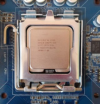
Pentium D is a range of desktop 64-bit x86-64 processors based on the NetBurst microarchitecture, which is the dual-core variant of the Pentium 4 manufactured by Intel. Each CPU comprised two cores. The brand's first processor, codenamed Smithfield and manufactured on the 90 nm process, was released on May 25, 2005, followed by the 65 nm Presler nine months later. The core implementation on the 90 nm "Smithfield" and later 65 nm "Presler" are designed differently but are functionally the same. The 90 nm "Smithfield" contains a single die, with two adjoined but functionally separate CPU cores cut from the same wafer. The later 65 nm "Presler" utilized a multi-chip module package, where two discrete dies each containing a single core reside on the CPU substrate. Neither the 90nm "Smithfield" nor the 65 nm "Presler" were capable of direct core to core communication, relying instead on the northbridge link to send information between the 2 cores.

<span class="mw-page-title-main">P6 (microarchitecture)</span> Intel processor microarchitecture

The P6 microarchitecture is the sixth-generation Intel x86 microarchitecture, implemented by the Pentium Pro microprocessor that was introduced in November 1995. It is frequently referred to as i686. It was planned to be succeeded by the NetBurst microarchitecture used by the Pentium 4 in 2000, but was revived for the Pentium M line of microprocessors. The successor to the Pentium M variant of the P6 microarchitecture is the Core microarchitecture which in turn is also derived from P6.

<span class="mw-page-title-main">Yonah (microprocessor)</span> Code name of Intels first generation 65 nm process CPU cores

Yonah is the code name of Intel's first generation 65 nm process CPU cores, based on cores of the earlier Banias / Dothan Pentium M microarchitecture. Yonah CPU cores were used within Intel's Core Solo and Core Duo mobile microprocessor products. SIMD performance on Yonah improved through the addition of SSE3 instructions and improvements to SSE and SSE2 implementations; integer performance decreased slightly due to higher latency cache. Additionally, Yonah included support for the NX bit.

<span class="mw-page-title-main">Intel Core 2</span> Processor family by Intel

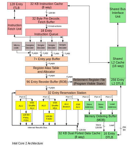
Intel Core 2 was a processor family encompassing a range of Intel's mainstream 64-bit x86-64 single-, dual-, and quad-core microprocessors based on the Core microarchitecture. The single- and dual-core models are single-die, whereas the quad-core models comprise two dies, each containing two cores, packaged in a multi-chip module. The Core 2 range was the last flagship range of Intel desktop processors to use a front-side bus (FSB).

<span class="mw-page-title-main">Pentium</span> Brand of discontinued microprocessors produced by Intel

Pentium is a discontinued series of x86 architecture-compatible microprocessors produced by Intel. The original Pentium was first released on March 22, 1993. The name "Pentium" is originally derived from the Greek word pente (πεντε), meaning "five", a reference to the prior numeric naming convention of Intel's 80x86 processors (8086–80486), with the Latin ending -ium since the processor would otherwise have been named 80586 using that convention.

<span class="mw-page-title-main">LGA 771</span>

LGA 771, also known as Socket J, is a CPU interface introduced by Intel in 2006. It is used in Intel Core microarchitecture and NetBurst microarchitecture (Dempsey) based DP-capable server processors, the Dual-Core Xeon is codenamed Dempsey, Woodcrest, and Wolfdale and the Quad-Core processors Clovertown, Harpertown, and Yorkfield-CL. It is also used for the Core 2 Extreme QX9775, and blade servers designated under Conroe-CL.

<span class="mw-page-title-main">Pentium Dual-Core</span> Line of CPUs by Intel

The Pentium Dual-Core brand was used for mainstream x86-architecture microprocessors from Intel from 2006 to 2009, when it was renamed to Pentium. The processors are based on either the 32-bit Yonah or 64-bit Merom-2M, Allendale, and Wolfdale-3M core, targeted at mobile or desktop computers.

<span class="mw-page-title-main">Conroe (microprocessor)</span> Code name for several Intel processors

Conroe is the code name for many Intel processors sold as Core 2 Duo, Xeon, Pentium Dual-Core and Celeron. It was the first desktop processor to be based on the Core microarchitecture, replacing the NetBurst microarchitecture based Cedar Mill processor. It has product code 80557, which is shared with Allendale and Conroe-L that are very similar but have a smaller L2 cache. Conroe-L has only one processor core and a new CPUID model. The mobile version of Conroe is Merom, the dual-socket server version is Woodcrest, the quad-core desktop version is Kentsfield and the quad-core dual-socket version is Clovertown. Conroe was replaced by the 45 nm Wolfdale processor.

<span class="mw-page-title-main">Merom (microprocessor)</span> Code name for various mobile Intel processors

Merom is the code name for various mobile Intel processors that are sold as Core 2 Duo, Core 2 Solo, Pentium Dual-Core and Celeron. It was the first mobile processor to be based on the Core microarchitecture, replacing the Enhanced Pentium M-based Yonah processor. Merom has the product code 80537, which is shared with Merom-2M and Merom-L that are very similar but have a smaller L2 cache. Merom-L has only one processor core and a different CPUID model. The desktop version of Merom is Conroe and the dual-socket server version is Woodcrest. Merom was manufactured in a 65 nanometer process, and was succeeded by Penryn, a 45 nm version of the Merom architecture. Together, Penryn and Merom represented the first 'tick-tock' in Intel's Tick-Tock manufacturing paradigm, in which Penryn was the 'tick' to Merom's 'tock'.

<span class="mw-page-title-main">Penryn (microprocessor)</span>

Penryn is the code name of a processor from Intel that is sold in varying configurations as Core 2 Solo, Core 2 Duo, Core 2 Quad, Pentium and Celeron.

<span class="mw-page-title-main">Wolfdale (microprocessor)</span>

Wolfdale is the code name for a processor from Intel that is sold in varying configurations as Core 2 Duo, Celeron, Pentium and Xeon. In Intel's Tick-Tock cycle, the 2007/2008 "Tick" was Penryn microarchitecture, the shrink of the Merom microarchitecture to 45 nanometers as CPUID model 23. This replaced the Conroe processor with Wolfdale.

<span class="mw-page-title-main">Yorkfield</span>

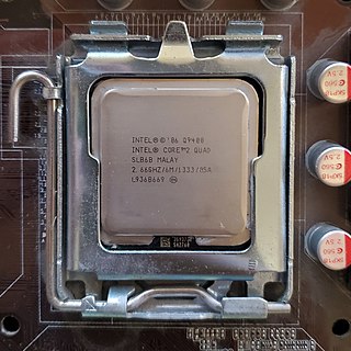
Yorkfield is the code name for some Intel processors sold as Core 2 Quad and Xeon. In Intel's Tick-Tock cycle, the 2007/2008 "Tick" was Penryn microarchitecture, the shrink of the Core microarchitecture to 45 nanometers as CPUID model 23, replacing Kentsfield, the previous model.

In Intel's Tick-Tock cycle, the 2007/2008 "Tick" was the shrink of the Core microarchitecture to 45 nanometers as CPUID model 23. In Core 2 processors, it is used with the code names Penryn, Wolfdale and Yorkfield, some of which are also sold as Celeron, Pentium and Xeon processors. In the Xeon brand, the Wolfdale-DP and Harpertown code names are used for LGA 771 based MCMs with two or four active Wolfdale cores.

References

  1. NetBurst had reached 3.8 GHz in 2004. Core initially reached 3 GHz, and after moving to 45nm in Penryn would reach 3.5 GHz. Westmere, the ultimate evolution of P6, reached 3.6 GHz base and 3.86 GHz boost frequency. (Excluding the 4.4 GHz special-order Xeons.)
  2. 77 mm² according to Intel, [14] 80 mm² according to Hiroshige Goto [15]
  1. Bessonov, Oleg (September 9, 2005). "New Wine into Old Skins. Conroe: Grandson of Pentium III, Nephew of NetBurst?". ixbtlabs.com. Note that all mentions of "Next-Generation Micro-architecture" in Intel's slides have asterisks that warn that "micro-architecture name TBD".
  2. 1 2 Hinton, Glenn (February 17, 2010). "Key Nehalem Choices" (PDF).
  3. "Intel cancels Tejas, moves to dual-core designs". EE Times . May 7, 2004.
  4. "Penryn Arrives: Core 2 Extreme QX9650 Review". ExtremeTech. Archived from the original on October 31, 2007. Retrieved October 30, 2006.
  5. King, Ian (April 9, 2007). "How Israel saved Intel". The Seattle Times. Retrieved April 15, 2012.
  6. "Driving energy-efficient performance, innovation with Intel Core microarchitecture" (PDF). Intel. March 7, 2006.
  7. De Gelas, Johan. "The Bulldozer Aftermath: Delving Even Deeper". AnandTech .
  8. Thomadakis, Michael Euaggelos. "The Architecture of the Nehalem Processor and Nehalem-EP SMP Platforms".
  9. De Gelas, Johan. "Intel Core versus AMD's K8 architecture". AnandTech .
  10. "Intel Xeon Processor 5110". Intel. Retrieved April 15, 2012.
  11. "Intel Xeon Processor 5120". Intel. Retrieved April 15, 2012.
  12. "Intel Core 2 Extreme QX9650 - Penryn Ticks Ahead".
  13. "Intel Core 2 Duo Mobile Processors T7400 & L7400 and Intel Celeron M Processor 530 (Merom - Napa Refresh), PCN 108529-03, Product Design, B-2 to G-2 Stepping Conversion, Reason for Revision: Change G-0 to G-2 Stepping and Correct Post Conversion MM#" (PDF). Intel. March 30, 2009.
  14. Intel® Celeron® Processor 440 ark.intel.com
  15. Intel CPU Die-Size and Microarchitecture
  16. "Product Change Notice" (PDF). Archived from the original (PDF) on December 22, 2010. Retrieved June 17, 2012.
  17. "ARK entry for Intel Xeon Processor X7460". Intel. Retrieved July 14, 2009.
  18. piotke (August 1, 2006). "Intel Core 2: Is high speed memory worth its price?". Madshrimps. Retrieved August 1, 2006.
  19. Jacob (May 19, 2007). "Benchmarks of four Prime95 processes on a quad-core". Mersenne Forum. Retrieved May 22, 2007.
  20. "Dual-Core Intel Xeon Processor 7200 Series and Quad-Core Intel Xeon Processor 7300 Series" (PDF). p. 46. Retrieved January 23, 2010.
  21. "Intel Core 2 Duo Processor for Intel Centrino Duo Processor Technology Specification Update" (PDF). pp. 18–21.
  22. "'Intel Core 2' - MARC". marc.info.
  23. "Matthew Dillon on Intel Core Bugs". OpenBSD journal. June 30, 2007. Retrieved April 15, 2012.
  24. Torvalds, Linus (June 27, 2007). "Core 2 Errata -- problematic or overblown?". Real World Technologies. Retrieved April 15, 2012.
  25. "A microcode reliability update is available that improves the reliability of systems that use Intel processors". Microsoft. October 8, 2011. Retrieved April 15, 2012.