In physics, sputtering is a phenomenon in which microscopic particles of a solid material are ejected from its surface, after the material is itself bombarded by energetic particles of a plasma or gas. It occurs naturally in outer space, and can be an unwelcome source of wear in precision components. However, the fact that it can be made to act on extremely fine layers of material is utilised in science and industry—there, it is used to perform precise etching, carry out analytical techniques, and deposit thin film layers in the manufacture of optical coatings, semiconductor devices and nanotechnology products. It is a physical vapor deposition technique.

A flashtube (flashlamp) produces an electrostatic discharge with an extremely intense, incoherent, full-spectrum white light for a very short time. A flashtube is a glass tube with an electrode at each end and is filled with a gas that, when triggered, ionizes and conducts a high-voltage pulse to make light. Flashtubes are used most in photography; they also are used in science, medicine, industry, and entertainment.

Pulsed laser deposition (PLD) is a physical vapor deposition (PVD) technique where a high-power pulsed laser beam is focused inside a vacuum chamber to strike a target of the material that is to be deposited. This material is vaporized from the target which deposits it as a thin film on a substrate. This process can occur in ultra high vacuum or in the presence of a background gas, such as oxygen which is commonly used when depositing oxides to fully oxygenate the deposited films.

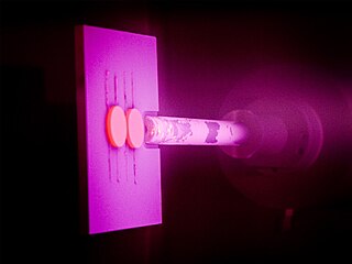
A glow discharge is a plasma formed by the passage of electric current through a gas. It is often created by applying a voltage between two electrodes in a glass tube containing a low-pressure gas. When the voltage exceeds a value called the striking voltage, the gas ionization becomes self-sustaining, and the tube glows with a colored light. The color depends on the gas used.

An electric arc is an electrical breakdown of a gas that produces a prolonged electrical discharge. The current through a normally nonconductive medium such as air produces a plasma, which may produce visible light. An arc discharge is initiated either by thermionic emission or by field emission. After initiation, the arc relies on thermionic emission of electrons from the electrodes supporting the arc. An arc discharge is characterized by a lower voltage than a glow discharge. An archaic term is voltaic arc, as used in the phrase "voltaic arc lamp".
A vacuum arc can arise when the surfaces of metal electrodes in contact with a good vacuum begin to emit electrons either through heating or in an electric field that is sufficient to cause field electron emission. Once initiated, a vacuum arc can persist, since the freed particles gain kinetic energy from the electric field, heating the metal surfaces through high-speed particle collisions. This process can create an incandescent cathode spot, which frees more particles, thereby sustaining the arc. At sufficiently high currents an incandescent anode spot may also be formed.
Cathodic arc deposition or Arc-PVD is a physical vapor deposition technique in which an electric arc is used to vaporize material from a cathode target. The vaporized material then condenses on a substrate, forming a thin film. The technique can be used to deposit metallic, ceramic, and composite films.

Ion plating (IP) is a physical vapor deposition (PVD) process that is sometimes called ion assisted deposition (IAD) or ion vapor deposition (IVD) and is a modified version of vacuum deposition. Ion plating uses concurrent or periodic bombardment of the substrate, and deposits film by atomic-sized energetic particles called ions. Bombardment prior to deposition is used to sputter clean the substrate surface. During deposition the bombardment is used to modify and control the properties of the depositing film. It is important that the bombardment be continuous between the cleaning and the deposition portions of the process to maintain an atomically clean interface. If this interface is not properly cleaned, then it can result into a weaker coating or poor adhesion.
Vacuum deposition is a group of processes used to deposit layers of material atom-by-atom or molecule-by-molecule on a solid surface. These processes operate at pressures well below atmospheric pressure. The deposited layers can range from a thickness of one atom up to millimeters, forming freestanding structures. Multiple layers of different materials can be used, for example to form optical coatings. The process can be qualified based on the vapor source; physical vapor deposition uses a liquid or solid source and chemical vapor deposition uses a chemical vapor.
Physical vapor deposition (PVD), sometimes called physical vapor transport (PVT), describes a variety of vacuum deposition methods which can be used to produce thin films and coatings on substrates including metals, ceramics, glass, and polymers. PVD is characterized by a process in which the material transitions from a condensed phase to a vapor phase and then back to a thin film condensed phase. The most common PVD processes are sputtering and evaporation. PVD is used in the manufacturing of items which require thin films for optical, mechanical, electrical, acoustic or chemical functions. Examples include semiconductor devices such as thin-film solar cells, microelectromechanical devices such as thin film bulk acoustic resonator, aluminized PET film for food packaging and balloons, and titanium nitride coated cutting tools for metalworking. Besides PVD tools for fabrication, special smaller tools used mainly for scientific purposes have been developed.
Plasma activation is a method of surface modification employing plasma processing, which improves surface adhesion properties of many materials including metals, glass, ceramics, a broad range of polymers and textiles and even natural materials such as wood and seeds. Plasma functionalization also refers to the introduction of functional groups on the surface of exposed materials. It is widely used in industrial processes to prepare surfaces for bonding, gluing, coating and painting. Plasma processing achieves this effect through a combination of reduction of metal oxides, ultra-fine surface cleaning from organic contaminants, modification of the surface topography and deposition of functional chemical groups. Importantly, the plasma activation can be performed at atmospheric pressure using air or typical industrial gases including hydrogen, nitrogen and oxygen. Thus, the surface functionalization is achieved without expensive vacuum equipment or wet chemistry, which positively affects its costs, safety and environmental impact. Fast processing speeds further facilitate numerous industrial applications.

Plasma-enhanced chemical vapor deposition (PECVD) is a chemical vapor deposition process used to deposit thin films from a gas state (vapor) to a solid state on a substrate. Chemical reactions are involved in the process, which occur after creation of a plasma of the reacting gases. The plasma is generally created by radio frequency (RF) alternating current (AC) frequency or direct current (DC) discharge between two electrodes, the space between which is filled with the reacting gases.

An ion pump is a type of vacuum pump which operates by sputtering a metal getter. Under ideal conditions, ion pumps are capable of reaching pressures as low as 10−11 mbar. An ion pump first ionizes gas within the vessel it is attached to and employs a strong electrical potential, typically 3–7 kV, which accelerates the ions into a solid electrode. Small bits of the electrode are sputtered into the chamber. Gasses are trapped by a combination of chemical reactions with the surface of the highly-reactive sputtered material, and being physically trapped underneath that material.

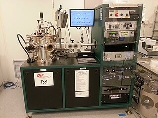
Sputter deposition is a physical vapor deposition (PVD) method of thin film deposition by the phenomenon of sputtering. This involves ejecting material from a "target" that is a source onto a "substrate" such as a silicon wafer. Resputtering is re-emission of the deposited material during the deposition process by ion or atom bombardment. Sputtered atoms ejected from the target have a wide energy distribution, typically up to tens of eV. The sputtered ions can ballistically fly from the target in straight lines and impact energetically on the substrates or vacuum chamber. Alternatively, at higher gas pressures, the ions collide with the gas atoms that act as a moderator and move diffusively, reaching the substrates or vacuum chamber wall and condensing after undergoing a random walk. The entire range from high-energy ballistic impact to low-energy thermalized motion is accessible by changing the background gas pressure. The sputtering gas is often an inert gas such as argon. For efficient momentum transfer, the atomic weight of the sputtering gas should be close to the atomic weight of the target, so for sputtering light elements neon is preferable, while for heavy elements krypton or xenon are used. Reactive gases can also be used to sputter compounds. The compound can be formed on the target surface, in-flight or on the substrate depending on the process parameters. The availability of many parameters that control sputter deposition make it a complex process, but also allow experts a large degree of control over the growth and microstructure of the film.
High-power impulse magnetron sputtering is a method for physical vapor deposition of thin films which is based on magnetron sputter deposition. HIPIMS utilises extremely high power densities of the order of kW⋅cm−2 in short pulses (impulses) of tens of microseconds at low duty cycle of < 10%. Distinguishing features of HIPIMS are a high degree of ionisation of the sputtered metal and a high rate of molecular gas dissociation which result in high density of deposited films. The ionization and dissociation degree increase according to the peak cathode power. The limit is determined by the transition of the discharge from glow to arc phase. The peak power and the duty cycle are selected so as to maintain an average cathode power similar to conventional sputtering (1–10 W⋅cm−2).

Plasma-immersion ion implantation (PIII) or pulsed-plasma doping is a surface modification technique of extracting the accelerated ions from the plasma by applying a high voltage pulsed DC or pure DC power supply and targeting them into a suitable substrate or electrode with a semiconductor wafer placed over it, so as to implant it with suitable dopants. The electrode is a cathode for an electropositive plasma, while it is an anode for an electronegative plasma. Plasma can be generated in a suitably designed vacuum chamber with the help of various plasma sources such as electron cyclotron resonance plasma source which yields plasma with the highest ion density and lowest contamination level, helicon plasma source, capacitively coupled plasma source, inductively coupled plasma source, DC glow discharge and metal vapor arc. The vacuum chamber can be of two types - diode and triode type depending upon whether the power supply is applied to the substrate as in the former case or to the perforated grid as in the latter.
A microplasma is a plasma of small dimensions, ranging from tens to thousands of micrometers. Microplasmas can be generated at a variety of temperatures and pressures, existing as either thermal or non-thermal plasmas. Non-thermal microplasmas that can maintain their state at standard temperatures and pressures are readily available and accessible to scientists as they can be easily sustained and manipulated under standard conditions. Therefore, they can be employed for commercial, industrial, and medical applications, giving rise to the evolving field of microplasmas.

Ivan Georgiev Petrov is a Bulgarian-American physicist specializing in thin films, surface science, and methods of characterization of materials. His research and scientific contributions have been described as having an "enormous impact on the hard-coatings community". Petrov was the president of the American Vacuum Society for 2015.
Paul André Albert was an American metallurgist. In the 1970s and 1980s, he helped to develop the class of doped cobalt-chrome alloys still in use in the manufacture of computer hard disks.

Edl Schamiloglu is an American physicist, electrical engineer, pulsed power expert, inventor, and distinguished professor in the department of electrical and computer engineering at the University of New Mexico. He has been known in public media for his expertise in the design and operation of directed-energy weapons. He is also known for his assessment on the possible origins of alleged health damages presumably caused on U.S. embassy personnel in Cuba in 2016 as part of the Havana syndrome incident. He is the associate dean for research and innovation at the UNM School of Engineering, where he has been a faculty since 1988, and where he is also special assistant to the provost for laboratory relations. He is also the founding director of the recently launched UNM Directed Energy Center. Schamiloglu is a book author and co-editor, and has received numerous awards for his academic achievements. He is a Fellow of the Institute of Electrical and Electronics Engineers and the American Physical Society. Starting on July 1, 2024, Schamiloglu was selected as Editor-in-Chief of the IEEE Transactions on Plasma Science, where he succeeds Steven J. Gitomer who has held that role for over 40 years.
