A diode is a two-terminal electronic component that conducts current primarily in one direction. It has low resistance in one direction, and high resistance in the other.

An integrated circuit is a set of electronic circuits on one small flat piece of semiconductor material, usually silicon. Large numbers of miniaturized transistors and other electronic components are integrated together on the chip. This results in circuits that are orders of magnitude smaller, faster, and less expensive than those constructed of discrete components, allowing a large transistor count.

MEMS is the technology of microscopic devices incorporating both electronic and moving parts. MEMS are made up of components between 1 and 100 micrometres in size, and MEMS devices generally range in size from 20 micrometres to a millimetre, although components arranged in arrays can be more than 1000 mm2. They usually consist of a central unit that processes data and several components that interact with the surroundings.

A transistor is a semiconductor device used to amplify or switch electrical signals and power. It is one of the basic building blocks of modern electronics. It is composed of semiconductor material, usually with at least three terminals for connection to an electronic circuit. A voltage or current applied to one pair of the transistor's terminals controls the current through another pair of terminals. Because the controlled (output) power can be higher than the controlling (input) power, a transistor can amplify a signal. Some transistors are packaged individually, but many more in miniature form are found embedded in integrated circuits. Because transistors are the key active components in practically all modern electronics, many people consider them one of the 20th century's greatest inventions.

A semiconductor device is an electronic component that relies on the electronic properties of a semiconductor material for its function. Its conductivity lies between conductors and insulators. Semiconductor devices have replaced vacuum tubes in most applications. They conduct electric current in the solid state, rather than as free electrons across a vacuum or as free electrons and ions through an ionized gas.

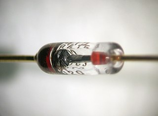
The Schottky diode, also known as Schottky barrier diode or hot-carrier diode, is a semiconductor diode formed by the junction of a semiconductor with a metal. It has a low forward voltage drop and a very fast switching action. The cat's-whisker detectors used in the early days of wireless and metal rectifiers used in early power applications can be considered primitive Schottky diodes.
A power semiconductor device is a semiconductor device used as a switch or rectifier in power electronics. Such a device is also called a power device or, when used in an integrated circuit, a power IC.

Warren Palmer Waters was an American physicist, electrical engineer, and semiconductor pioneer. He filed several device and process patents in the field of solid state engineering and was the manager of the solid state research center for the Hughes Aircraft Company. Walter's innovative circuit designs led to the success of NASA's Surveyor program.
In semiconductor electronics fabrication technology, a self-aligned gate is a transistor manufacturing approach whereby the gate electrode of a MOSFET is used as a mask for the doping of the source and drain regions. This technique ensures that the gate is naturally and precisely aligned to the edges of the source and drain.
A transistor is a semiconductor device with at least three terminals for connection to an electric circuit. In the common case, the third terminal controls the flow of current between the other two terminals. This can be used for amplification, as in the case of a radio receiver, or for rapid switching, as in the case of digital circuits. The transistor replaced the vacuum-tube triode, also called a (thermionic) valve, which was much larger in size and used significantly more power to operate. The first transistor was successfully demonstrated on December 23, 1947, at Bell Laboratories in Murray Hill, New Jersey. Bell Labs was the research arm of American Telephone and Telegraph (AT&T). The three individuals credited with the invention of the transistor were William Shockley, John Bardeen and Walter Brattain. The introduction of the transistor is often considered one of the most important inventions in history.

A radio-frequency microelectromechanical system is a microelectromechanical system with electronic components comprising moving sub-millimeter-sized parts that provide radio-frequency (RF) functionality. RF functionality can be implemented using a variety of RF technologies. Besides RF MEMS technology, III-V compound semiconductor, ferrite, ferroelectric, silicon-based semiconductor, and vacuum tube technology are available to the RF designer. Each of the RF technologies offers a distinct trade-off between cost, frequency, gain, large-scale integration, lifetime, linearity, noise figure, packaging, power handling, power consumption, reliability, ruggedness, size, supply voltage, switching time and weight.
In solid-state physics, a metal–semiconductor (M–S) junction is a type of electrical junction in which a metal comes in close contact with a semiconductor material. It is the oldest practical semiconductor device. M–S junctions can either be rectifying or non-rectifying. The rectifying metal–semiconductor junction forms a Schottky barrier, making a device known as a Schottky diode, while the non-rectifying junction is called an ohmic contact.
Baker clamp is a generic name for a class of electronic circuits that reduce the storage time of a switching bipolar junction transistor (BJT) by applying a nonlinear negative feedback through various kinds of diodes. The reason for slow turn-off times of saturated BJTs is the stored charge in the base. It must be removed before the transistor will turn off since the storage time is a limiting factor of using bipolar transistors and IGBTs in fast switching applications. The diode-based Baker clamps prevent the transistor from saturating and thereby accumulating a lot of stored charge.
An optical rectenna is a rectenna that works with visible or infrared light. A rectenna is a circuit containing an antenna and a diode, which turns electromagnetic waves into direct current electricity. While rectennas have long been used for radio waves or microwaves, an optical rectenna would operate the same way but with infrared or visible light, turning it into electricity.

A Schottky transistor is a combination of a transistor and a Schottky diode that prevents the transistor from saturating by diverting the excessive input current. It is also called a Schottky-clamped transistor.
The first planar monolithic integrated circuit (IC) chip was demonstrated in 1960. The idea of integrating electronic circuits into a single device was born when the German physicist and engineer Werner Jacobi developed and patented the first known integrated transistor amplifier in 1949 and the British radio engineer Geoffrey Dummer proposed to integrate a variety of standard electronic components in a monolithic semiconductor crystal in 1952. A year later, Harwick Johnson filed a patent for a prototype IC. Between 1953 and 1957, Sidney Darlington and Yasuo Tarui proposed similar chip designs where several transistors could share a common active area, but there was no electrical isolation to separate them from each other.
Dawon Kahng was a Korean-American electrical engineer and inventor, known for his work in solid-state electronics. He is best known for inventing the MOSFET, along with his colleague Mohamed Atalla, in 1959. Kahng and Atalla developed both the PMOS and NMOS processes for MOSFET semiconductor device fabrication. The MOSFET is the most widely used type of transistor, and the basic element in most modern electronic equipment.
Mohamed M. Atalla was an Egyptian-American engineer, physicist, cryptographer, inventor and entrepreneur. He was a semiconductor pioneer who made important contributions to modern electronics. He is best known for the first working demonstration of the MOSFET in 1959, which along with Atalla's earlier surface passivation processes, had a significant impact on the development of the electronics industry. He is also known as the founder of the data security company Atalla Corporation, founded in 1972. He received the Stuart Ballantine Medal and was inducted into the National Inventors Hall of Fame for his important contributions to semiconductor technology as well as data security.
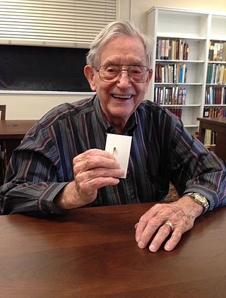
James Robert Biard was an American electrical engineer and inventor who held 73 U.S. patents. Some of his more significant patents include the first infrared light-emitting diode (LED), the optical isolator, Schottky clamped logic circuits, silicon Metal Oxide Semiconductor Read Only Memory, a low bulk leakage current avalanche photodetector, and fiber-optic data links. In 1980, Biard became a member of the staff of Texas A&M University as an Adjunct Professor of Electrical Engineering. In 1991, he was elected as a member into the National Academy of Engineering for contributions to semiconductor light-emitting diodes and lasers, Schotky-clamped logic, and read-only memories.

The field-effect transistor (FET) is a type of transistor that uses an electric field to control the flow of current in a semiconductor. It comes in two types: junction-gate FET (JFET) and metal-oxide-semiconductor FET (MOSFET). FETs have three terminals: source, gate, and drain. FETs control the flow of current by the application of a voltage to the gate, which in turn alters the conductivity between the drain and source.
