Related Research Articles

Microelectromechanical systems (MEMS), also written as micro-electro-mechanical systems and the related micromechatronics and microsystems constitute the technology of microscopic devices, particularly those with moving parts. They merge at the nanoscale into nanoelectromechanical systems (NEMS) and nanotechnology. MEMS are also referred to as micromachines in Japan and microsystem technology (MST) in Europe.

Semiconductor device fabrication is the process used to manufacture semiconductor devices, typically integrated circuit (IC) chips such as modern computer processors, microcontrollers, and memory chips such as NAND flash and DRAM that are present in everyday electrical and electronic devices. It is a multiple-step sequence of photolithographic and chemical processing steps during which electronic circuits are gradually created on a wafer made of pure semiconducting material. Silicon is almost always used, but various compound semiconductors are used for specialized applications.

In electronics, a wafer is a thin slice of semiconductor, such as a crystalline silicon (c-Si), used for the fabrication of integrated circuits and, in photovoltaics, to manufacture solar cells. The wafer serves as the substrate for microelectronic devices built in and upon the wafer. It undergoes many microfabrication processes, such as doping, ion implantation, etching, thin-film deposition of various materials, and photolithographic patterning. Finally, the individual microcircuits are separated by wafer dicing and packaged as an integrated circuit.
Passivation, in physical chemistry and engineering, refers to coating a material so it becomes "passive," that is, less readily affected or corroded by the environment. Passivation involves creation of an outer layer of shield material that is applied as a microcoating, created by chemical reaction with the base material, or allowed to build by spontaneous oxidation in the air. As a technique, passivation is the use of a light coat of a protective material, such as metal oxide, to create a shield against corrosion. Passivation of silicon is used during fabrication of microelectronic devices. In electrochemical treatment of water, passivation reduces the effectiveness of the treatment by increasing the circuit resistance, and active measures are typically used to overcome this effect, the most common being polarity reversal, which results in limited rejection of the fouling layer.

Epitaxy refers to a type of crystal growth or material deposition in which new crystalline layers are formed with one or more well-defined orientations with respect to the crystalline seed layer. The deposited crystalline film is called an epitaxial film or epitaxial layer. The relative orientation(s) of the epitaxial layer to the seed layer is defined in terms of the orientation of the crystal lattice of each material. For most epitaxial growths, the new layer is usually crystalline and each crystallographic domain of the overlayer must have a well-defined orientation relative to the substrate crystal structure. Epitaxy can involve single-crystal structures, although grain-to-grain epitaxy has been observed in granular films. For most technological applications, single domain epitaxy, which is the growth of an overlayer crystal with one well-defined orientation with respect to the substrate crystal, is preferred. Epitaxy can also play an important role while growing superlattice structures.
Silicon on sapphire (SOS) is a hetero-epitaxial process for metal-oxide-semiconductor (MOS) integrated circuit (IC) manufacturing that consists of a thin layer (typically thinner than 0.6 µm) of silicon grown on a sapphire (Al2O3) wafer. SOS is part of the silicon-on-insulator (SOI) family of CMOS (complementary MOS) technologies.
In semiconductor manufacturing, silicon on insulator (SOI) technology is fabrication of silicon semiconductor devices in a layered silicon–insulator–silicon substrate, to reduce parasitic capacitance within the device, thereby improving performance. SOI-based devices differ from conventional silicon-built devices in that the silicon junction is above an electrical insulator, typically silicon dioxide or sapphire. The choice of insulator depends largely on intended application, with sapphire being used for high-performance radio frequency (RF) and radiation-sensitive applications, and silicon dioxide for diminished short-channel effects in other microelectronics devices. The insulating layer and topmost silicon layer also vary widely with application.

The planar process is a manufacturing process used in the semiconductor industry to build individual components of a transistor, and in turn, connect those transistors together. It is the primary process by which silicon integrated circuit chips are built. The process utilizes the surface passivation and thermal oxidation methods.
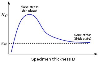
In materials science, fracture toughness is the critical stress intensity factor of a sharp crack where propagation of the crack suddenly becomes rapid and unlimited. A component's thickness affects the constraint conditions at the tip of a crack with thin components having plane stress conditions and thick components having plane strain conditions. Plane strain conditions give the lowest fracture toughness value which is a material property. The critical value of stress intensity factor in mode I loading measured under plane strain conditions is known as the plane strain fracture toughness, denoted . When a test fails to meet the thickness and other test requirements that are in place to ensure plane strain conditions, the fracture toughness value produced is given the designation . Fracture toughness is a quantitative way of expressing a material's resistance to crack propagation and standard values for a given material are generally available.

Geotechnical investigations are performed by geotechnical engineers or engineering geologists to obtain information on the physical properties of soil earthworks and foundations for proposed structures and for repair of distress to earthworks and structures caused by subsurface conditions. This type of investigation is called a site investigation. Additionally, geotechnical investigations are also used to measure the thermal resistivity of soils or backfill materials required for underground transmission lines, oil and gas pipelines, radioactive waste disposal, and solar thermal storage facilities. A geotechnical investigation will include surface exploration and subsurface exploration of a site. Sometimes, geophysical methods are used to obtain data about sites. Subsurface exploration usually involves soil sampling and laboratory tests of the soil samples retrieved.
In the context of manufacturing integrated circuits, wafer dicing is the process by which die are separated from a wafer of semiconductor following the processing of the wafer. The dicing process can involve scribing and breaking, mechanical sawing or laser cutting. All methods are typically automated to ensure precision and accuracy. Following the dicing process the individual silicon chips are encapsulated into chip carriers which are then suitable for use in building electronic devices such as computers, etc.
Surface photovoltage (SPV) measurements are a widely used method to determine the minority carrier diffusion length of semiconductors. Since the transport of minority carriers determines the behavior of the p-n junctions that are ubiquitous in semiconductor devices, surface photovoltage data can be very helpful in understanding their performance. As a contactless method, SPV is a popular technique for characterizing poorly understood compound semiconductors where the fabrication of ohmic contacts or special device structures may be difficult.
Monocrystalline silicon, more often called single-crystal silicon, in short mono c-Si or mono-Si, is the base material for silicon-based discrete components and integrated circuits used in virtually all modern electronic equipment. Mono-Si also serves as a photovoltaic, light-absorbing material in the manufacture of solar cells.

In the paint and coating industries, paint adhesion testing is often used to determine if the paint or coating will adhere properly to the substrates to which they are applied. There are several different tests to measure the resistance of paints and coatings from substrates: cross-cut test, scrape adhesion, pull-off test, and others.

Mixed flowing gas (MFG) is a type of laboratory environmental testing for products, particularly electronics, to evaluate resistance to corrosion due to gases in the atmosphere. Mixed Flowing Gas (MFG) test is a laboratory test in which the temperature (°C), relative humidity (%RH), concentration of gaseous pollutants, and other critical variables are carefully defined, monitored and controlled. The purpose of this test is to simulate corrosion phenomenon due to atmospheric exposure. The electronic product is exposed to gases such as chlorine, hydrogen sulfide, nitrogen dioxide, and sulfur dioxide at levels in the parts per billion range, in a controlled environmental chamber. Test samples that have been exposed to MFG testing have ranged from bare metal surfaces, to electrical connectors, and to complete assemblies. In regards to noble metal plated connector applications, MFG testing has been widely accepted as a qualification test method to evaluate the performance of these connectors.
Simply stated, Klaiber's law proposes that "the silicon wafer size will dictate the largest diameter of ultrapure water supply piping needed within a semiconductor wafer factory."

Tensile testing, also known as tension testing, is a fundamental materials science and engineering test in which a sample is subjected to a controlled tension until failure. Properties that are directly measured via a tensile test are ultimate tensile strength, breaking strength, maximum elongation and reduction in area. From these measurements the following properties can also be determined: Young's modulus, Poisson's ratio, yield strength, and strain-hardening characteristics. Uniaxial tensile testing is the most commonly used for obtaining the mechanical characteristics of isotropic materials. Some materials use biaxial tensile testing. The main difference between these testing machines being how load is applied on the materials.
Ultrapure water (UPW), high-purity water or highly purified water (HPW) is water that has been purified to uncommonly stringent specifications. Ultrapure water is a term commonly used in manufacturing to emphasize the fact that the water is treated to the highest levels of purity for all contaminant types, including: organic and inorganic compounds; dissolved and particulate matter; volatile and non-volatile; reactive, and inert; hydrophilic and hydrophobic; and dissolved gases.

Photolithography is a process in removing select portions of thin films used in microfabrication. Microfabrication is the production of parts on the micro- and nano- scale, typically on the surface of silicon wafers, for the production of integrated circuits, microelectromechanical systems (MEMS), solar cells, and other devices. Photolithography makes this process possible through the combined use of hexamethyldisilazane (HMDS), photoresist, spin coating, photomask, an exposure system and other various chemicals. By carefully manipulating these factors it is possible to create nearly any geometry microstructure on the surface of a silicon wafer. The chemical interaction between all the different components and the surface of the silicon wafer makes photolithography an interesting chemistry problem. Current engineering has been able to create features on the surface of silicon wafers between 1 and 100 μm.
Floor slip resistance testing is the science of measuring the coefficient of friction of flooring surfaces, either in a laboratory or on floors in situ. Slip resistance testing is usually desired by the building's owner or manager when there has been a report of a slip and fall accident, when there has been a report of a near accident, or (preferably) before the flooring is installed on the property. Flooring is tested using a tribometer to discover if there is a high propensity for slip and fall accidents on it, either dry and/or when wet with water or lubricated with other contaminants such as kitchen grease, hydraulic oil, etc. There have been numerous floor slip resistance testing tribometers and lab devices produced around the world to measure both the static (stationary) and dynamic coefficient of friction, but presently there are only a few that have been proven to be reliable for obtaining useful safety results and that have current official test methods. Static coefficient of friction (SCOF) testing has always been unreliable for assessing safety in the wet condition, so any reliable slip resistance test will be measuring the available slip resistance to someone who is moving (dynamic) across the floor, and therefore will be assessing dynamic coefficient of friction (DCOF). If an instrument has no official published test method, or has a withdrawn test method, then there is a problem with the instrument, often being poor precision.
References
- ↑ "ASTM F534 - 02a Standard Test Method for Bow of Silicon Wafers (Withdrawn 2003)". www.astm.org.
- ↑ "ASTM F657 - 92(1999) Standard Test Method for Measuring Warp and Total Thickness Variation on Silicon Wafers by Noncontact Scanning (Withdrawn 2003)". www.astm.org.
- ↑ "ASTM F1390 - 02 Standard Test Method for Measuring Warp on Silicon Wafers by Automated Noncontact Scanning (Withdrawn 2003)". www.astm.org.
- ↑ [ permanent dead link ]
- ↑ "Optoprofiler". www.zebraoptical.com.
- ↑ Semiconductor measurements and instrumentation WR Runyan, 1975 - McGraw-Hill Companies
- ↑ "Archived copy" (PDF). Archived from the original (PDF) on 2009-02-20. Retrieved 2009-11-11.
{{cite web}}: CS1 maint: archived copy as title (link) - ↑ http://www.iop.org/EJ/abstract/0957-0233/19/2/025302 [ dead link ]