Related Research Articles
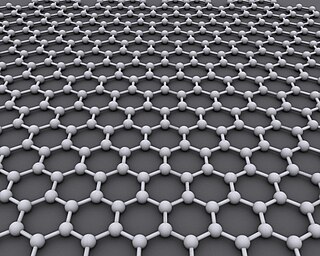
Graphene is an allotrope of carbon consisting of a single layer of atoms arranged in a hexagonal lattice nanostructure. The name is derived from "graphite" and the suffix -ene, reflecting the fact that the graphite allotrope of carbon contains numerous double bonds.

Phosphorene is a two-dimensional material consisting of phosphorus. It consists of a single layer of the artificially made layered black phosphorus, the most stable allotrope of phosphorus. The designation phosphorene has been introduced in analogy to the designation of graphene as a single layer of graphite. Among two-dimensional materials, phosphorene emerged as a strong competitor to graphene because, in contrast to graphene, phosphorene has a nonzero fundamental band gap that can be furthermore modulated by strain and the number of layers in a stack. Phosphorene was first isolated in 2014 by mechanical exfoliation.
Nanocomposite is a multiphase solid material where one of the phases has one, two or three dimensions of less than 100 nanometers (nm) or structures having nano-scale repeat distances between the different phases that make up the material.
Carbon nanotubes (CNTs) are cylinders of one or more layers of graphene (lattice). Diameters of single-walled carbon nanotubes (SWNTs) and multi-walled carbon nanotubes (MWNTs) are typically 0.8 to 2 nm and 5 to 20 nm, respectively, although MWNT diameters can exceed 100 nm. CNT lengths range from less than 100 nm to 0.5 m.

Nanobatteries are fabricated batteries employing technology at the nanoscale, particles that measure less than 100 nanometers or 10−7 meters. These batteries may be nano in size or may use nanotechnology in a macro scale battery. Nanoscale batteries can be combined to function as a macrobattery such as within a nanopore battery.
As the world's energy demand continues to grow, the development of more efficient and sustainable technologies for generating and storing energy is becoming increasingly important. According to Dr. Wade Adams from Rice University, energy will be the most pressing problem facing humanity in the next 50 years and nanotechnology has potential to solve this issue. Nanotechnology, a relatively new field of science and engineering, has shown promise to have a significant impact on the energy industry. Nanotechnology is defined as any technology that contains particles with one dimension under 100 nanometers in length. For scale, a single virus particle is about 100 nanometers wide.

Graphene nanoribbons are strips of graphene with width less than 100 nm. Graphene ribbons were introduced as a theoretical model by Mitsutaka Fujita and coauthors to examine the edge and nanoscale size effect in graphene.
Layer-by-layer (LbL) deposition is a thin film fabrication technique. The films are formed by depositing alternating layers of oppositely charged materials with wash steps in between. This can be accomplished by using various techniques such as immersion, spin, spray, electromagnetism, or fluidics.

Rodney S. "Rod" Ruoff is an American physical chemist and nanoscience researcher. He is one of the world experts on carbon materials including carbon nanostructures such as fullerenes, nanotubes, graphene, diamond, and has had pioneering discoveries on such materials and others. Ruoff received his B.S. in Chemistry from the University of Texas at Austin (1981) and his Ph.D. in Chemical Physics at the University of Illinois-Urbana (1988). After a Fulbright Fellowship at the MPI fuer Stroemungsforschung in Goettingen, Germany (1989) and postdoctoral work at the IBM T. J. Watson Research Center (1990–91), Ruoff became a staff scientist in the Molecular Physics Laboratory at SRI International (1991–1996). He is currently UNIST Distinguished Professor at the Ulsan National Institute of Science and Technology (UNIST), and the director of the Center for Multidimensional Carbon Materials, an Institute for Basic Science Center located at UNIST.

Nanocellulose is a term referring to nano-structured cellulose. This may be either cellulose nanocrystal, cellulose nanofibers (CNF) also called nanofibrillated cellulose (NFC), or bacterial nanocellulose, which refers to nano-structured cellulose produced by bacteria.
A potassium-ion battery or K-ion battery is a type of battery and analogue to lithium-ion batteries, using potassium ions for charge transfer instead of lithium ions. It was invented by the Iranian/American chemist Ali Eftekhari in 2004.

Nanoparticles are classified as having at least one of three dimensions be in the range of 1-100 nm. The small size of nanoparticles allows them to have unique characteristics which may not be possible on the macro-scale. Self-assembly is the spontaneous organization of smaller subunits to form larger, well-organized patterns. For nanoparticles, this spontaneous assembly is a consequence of interactions between the particles aimed at achieving a thermodynamic equilibrium and reducing the system’s free energy. The thermodynamics definition of self-assembly was introduced by Nicholas A. Kotov. He describes self-assembly as a process where components of the system acquire non-random spatial distribution with respect to each other and the boundaries of the system. This definition allows one to account for mass and energy fluxes taking place in the self-assembly processes.
A nanosheet is a two-dimensional nanostructure with thickness in a scale ranging from 1 to 100 nm.

Transition-metal dichalcogenide (TMD or TMDC) monolayers are atomically thin semiconductors of the type MX2, with M a transition-metal atom (Mo, W, etc.) and X a chalcogen atom (S, Se, or Te). One layer of M atoms is sandwiched between two layers of X atoms. They are part of the large family of so-called 2D materials, named so to emphasize their extraordinary thinness. For example, a MoS2 monolayer is only 6.5 Å thick. The key feature of these materials is the interaction of large atoms in the 2D structure as compared with first-row transition-metal dichalcogenides, e.g., WTe2 exhibits anomalous giant magnetoresistance and superconductivity.
A two-dimensional semiconductor is a type of natural semiconductor with thicknesses on the atomic scale. Geim and Novoselov et al. initiated the field in 2004 when they reported a new semiconducting material graphene, a flat monolayer of carbon atoms arranged in a 2D honeycomb lattice. A 2D monolayer semiconductor is significant because it exhibits stronger piezoelectric coupling than traditionally employed bulk forms. This coupling could enable applications. One research focus is on designing nanoelectronic components by the use of graphene as electrical conductor, hexagonal boron nitride as electrical insulator, and a transition metal dichalcogenide as semiconductor.
A rapidly increasing list of graphene production techniques have been developed to enable graphene's use in commercial applications.

Boron nitride nanosheet is a two-dimensional crystalline form of the hexagonal boron nitride (h-BN), which has a thickness of one to few atomic layers. It is similar in geometry as well as physical and thermal properties to its all-carbon analog graphene, but has very different chemical and electronic properties – contrary to the black and highly conducting graphene, BN nanosheets are electrical insulators with a band gap of ~5.9 eV, and therefore appear white in color.
Two dimensional hexagonal boron nitride is a material of comparable structure to graphene with potential applications in e.g. photonics., fuel cells and as a substrate for two-dimensional heterostructures. 2D h-BN is isostructural to graphene, but where graphene is conductive, 2D h-BN is a wide-gap insulator.
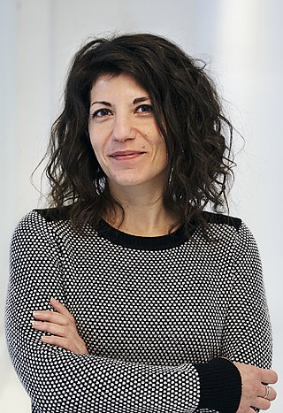
Raffaella Buonsanti (born 1981 in Matera, Italy) is an Italian chemist and material scientist. Her research is at the interface between materials chemistry and catalysis as she focuses on the synthesis of nanocrystals to drive various energy-related reactions, such as CO2 reduction. She is currently a tenure-track assistant professor at École Polytechnique Fédérale de Lausanne (EPFL) and director of the Laboratory of Nanochemistry for Energy located at EPFL's Valais campus.
The piezoelectrochemical transducer effect (PECT) is a coupling between the electrochemical potential and the mechanical strain in ion-insertion-based electrode materials. It is similar to the piezoelectric effect – with both exhibiting a voltage-strain coupling - although the PECT effect relies on movement of ions within a material microstructure, rather than charge accumulation from the polarization of electric dipole moments.
References
- ↑ Li, Q. L; X. Xie; L. Ju; X. F. Feng; Y. H. Sun; R. F. Zhou; K. Liu; S. S. Fan; K. L. Jiang (2009). "Controlled fabrication of high-quality carbon nanoscrolls from monolayer graphene". Nano Letters. 9 (7): 2565–2570. Bibcode:2009NanoL...9.2565X. doi:10.1021/nl900677y. PMID 19499895.
- ↑ Jayasena, B; Subbiah S; Reddy C.D (2014). "Formation of Carbon Nanoscrolls During Wedge-Based Mechanical Exfoliation of HOPG". Journal of Micro and Nano-Manufacturing. 2 (1): 011003. doi:10.1115/1.4026325.
- ↑ Kim, Jeong-Hwan; Benelmekki, Maria (2016). "Interfacial Transformation of an Amorphous Carbon Nanofilm upon Fe@Ag@Si Nanoparticle Landing and its Colloidal Nanoscrolls: Enhanced Nanocompositing-Based Performance for Bioapplications". ACS Applied Materials & Interfaces. 8 (48): 33121–33130. doi:10.1021/acsami.6b12993. ISSN 1944-8244. PMID 27934129.
- ↑ Kim, Jeong-Hwan; Bohra, Murtaza; Singh, Vidyadhar; Cassidy, Cathal; Sowwan, Mukhles (2014). "Smart Composite Nanosheets with Adaptive Optical Properties". ACS Applied Materials & Interfaces. 6 (16): 13339–13343. doi:10.1021/am5041708. ISSN 1944-8244. PMID 25116340.
- ↑ Kim, Jeong-Hwan; Lu, Tsai-Ming (2016). "Bio-inspired Janus composite nanoscrolls for on-demand tumour targeting". RSC Advances. 6 (21): 17179. Bibcode:2016RSCAd...617179K. doi:10.1039/C5RA27080D. ISSN 2046-2069.