Related Research Articles

MEMS is the technology of microscopic devices incorporating both electronic and moving parts. MEMS are made up of components between 1 and 100 micrometres in size, and MEMS devices generally range in size from 20 micrometres to a millimetre, although components arranged in arrays can be more than 1000 mm2. They usually consist of a central unit that processes data and several components that interact with the surroundings.
In integrated circuit manufacturing, photolithography or optical lithography is a general term used for techniques that use light to produce minutely patterned thin films of suitable materials over a substrate, such as a silicon wafer, to protect selected areas of it during subsequent etching, deposition, or implantation operations. Typically, ultraviolet light is used to transfer a geometric design from an optical mask to a light-sensitive chemical (photoresist) coated on the substrate. The photoresist either breaks down or hardens where it is exposed to light. The patterned film is then created by removing the softer parts of the coating with appropriate solvents, also known in this case as developers.

A photoresist is a light-sensitive material used in several processes, such as photolithography and photoengraving, to form a patterned coating on a surface. This process is crucial in the electronics industry.

Semiconductor device fabrication is the process used to manufacture semiconductor devices, typically integrated circuits (ICs) such as computer processors, microcontrollers, and memory chips that are present in everyday electrical and electronic devices. It is a multiple-step photolithographic and physio-chemical process during which electronic circuits are gradually created on a wafer, typically made of pure single-crystal semiconducting material. Silicon is almost always used, but various compound semiconductors are used for specialized applications.

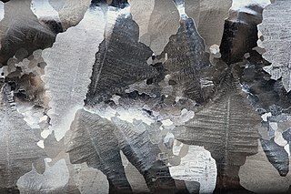
Etching is traditionally the process of using strong acid or mordant to cut into the unprotected parts of a metal surface to create a design in intaglio (incised) in the metal. In modern manufacturing, other chemicals may be used on other types of material. As a method of printmaking, it is, along with engraving, the most important technique for old master prints, and remains in wide use today. In a number of modern variants such as microfabrication etching and photochemical milling, it is a crucial technique in modern technology, including circuit boards.

A printed circuit board (PCB), also called printed wiring board (PWB), is a medium used to connect or "wire" components to one another in a circuit. It takes the form of a laminated sandwich structure of conductive and insulating layers: each of the conductive layers is designed with an artwork pattern of traces, planes and other features etched from one or more sheet layers of copper laminated onto and/or between sheet layers of a non-conductive substrate. Electrical components may be fixed to conductive pads on the outer layers in the shape designed to accept the component's terminals, generally by means of soldering, to both electrically connect and mechanically fasten them to it. Another manufacturing process adds vias: plated-through holes that allow interconnections between layers.

Rotogravure is a type of intaglio printing process, which involves engraving the image onto an image carrier. In gravure printing, the image is engraved onto a cylinder because, like offset printing and flexography, it uses a rotary printing press.

Photogravure is a process for printing photographs, also sometimes used for reproductive intaglio printmaking. It is a photo-mechanical process whereby a copper plate is grained and then coated with a light-sensitive gelatin tissue which had been exposed to a film positive, and then etched, resulting in a high quality intaglio plate that can reproduce detailed continuous tones of a photograph.
Dry etching refers to the removal of material, typically a masked pattern of semiconductor material, by exposing the material to a bombardment of ions that dislodge portions of the material from the exposed surface. A common type of dry etching is reactive-ion etching. Unlike with many of the wet chemical etchants used in wet etching, the dry etching process typically etches directionally or anisotropically.
Photoengraving is a process that uses a light-sensitive photoresist applied to the surface to be engraved to create a mask that protects some areas during a subsequent operation which etches, dissolves, or otherwise removes some or all of the material from the unshielded areas of a substrate. Normally applied to metal, it can also be used on glass, plastic and other materials.

Intaglio is the family of printing and printmaking techniques in which the image is incised into a surface and the incised line or sunken area holds the ink. It is the direct opposite of a relief print where the parts of the matrix that make the image stand above the main surface.
In semiconductor fabrication, a resist is a thin layer used to transfer a circuit pattern to the semiconductor substrate which it is deposited upon. A resist can be patterned via lithography to form a (sub)micrometer-scale, temporary mask that protects selected areas of the underlying substrate during subsequent processing steps. The material used to prepare said thin layer is typically a viscous solution. Resists are generally proprietary mixtures of a polymer or its precursor and other small molecules that have been specially formulated for a given lithography technology. Resists used during photolithography are called photoresists.

Etching is used in microfabrication to chemically remove layers from the surface of a wafer during manufacturing. Etching is a critically important process module, and every wafer undergoes many etching steps before it is complete.
A hardmask is a material used in semiconductor processing as an etch mask instead of a polymer or other organic "soft" resist material.
The lift-off process in microstructuring technology is a method of creating structures (patterning) of a target material on the surface of a substrate using a sacrificial material . It is an additive technique as opposed to more traditional subtracting technique like etching. The scale of the structures can vary from the nanoscale up to the centimeter scale or further, but are typically of micrometric dimensions.

Photochemical machining (PCM), also known as photochemical milling or photo etching, is a chemical milling process used to fabricate sheet metal components using a photoresist and etchants to corrosively machine away selected areas. This process emerged in the 1960s as an offshoot of the printed circuit board industry. Photo etching can produce highly complex parts with very fine detail accurately and economically.
Chemical milling or industrial etching is the subtractive manufacturing process of using baths of temperature-regulated etching chemicals to remove material to create an object with the desired shape. Other names for chemical etching include photo etching, chemical etching, photo chemical etching and photochemical machining. It is mostly used on metals, though other materials are increasingly important. It was developed from armor-decorating and printing etching processes developed during the Renaissance as alternatives to engraving on metal. The process essentially involves bathing the cutting areas in a corrosive chemical known as an etchant, which reacts with the material in the area to be cut and causes the solid material to be dissolved; inert substances known as maskants are used to protect specific areas of the material as resists.
A contact copier, is a device used to copy an image by illuminating a film negative with the image in direct contact with a photosensitive surface. The more common processes are negative, where clear areas in the original produce an opaque or hardened photosensitive surface, but positive processes are available. The light source is usually an actinic bulb internal or external to the device

A resist, used in many areas of manufacturing and art, is something that is added to parts of an object to create a pattern by protecting these parts from being affected by a subsequent stage in the process. Often the resist is then removed.
Polytetrafluoroethylene (PTFE), better known by its trade name Teflon, has many desirable properties which make it an attractive material for numerous industries. It has good chemical resistance, a low dielectric constant, low dielectric loss, and a low coefficient of friction, making it ideal for reactor linings, circuit boards, and kitchen utensils, to name a few applications. However, its nonstick properties make it challenging to bond to other materials or to itself.
References
- 1 2 3 4 "The Carbon Transfer Process". Archived from the original on 2013-09-18.
{{cite web}}: CS1 maint: bot: original URL status unknown (link) - ↑ Peres, Michael R. (29 May 2013). The Focal Encyclopedia of Photography. ISBN 9781136106132 . Retrieved 24 September 2013.
{{cite book}}:|work=ignored (help) - 1 2 3 "Carbon Transfer: Contemporary Printers". sandykingphotography.com. Archived from the original on 9 October 2013. Retrieved 9 October 2013.
{{cite web}}: CS1 maint: bot: original URL status unknown (link) - ↑ "DEFINITIONS OF PRINT PROCESSES". www.photoeye.com. Archived from the original on 23 March 2006. Retrieved 24 September 2013.
- ↑ "Gravure Engraving". Paul D. Fleming III, Paper Engineering, Chemical Engineering and Imaging. www.wmich.edu. Archived from the original on 17 October 2013. Retrieved 17 October 2013.
{{cite web}}: CS1 maint: bot: original URL status unknown (link) - ↑ James, Christopher (2015). The Book of Alternative Photographic Processes. Cengage Learning. pp. 583–584. ISBN 978-1-305-46159-8.