Chemical-mechanical planarization

Last updated

Chemical mechanical polishing/planarization is a process of smoothing surfaces with the combination of chemical and mechanical forces. It can be thought of as a hybrid of chemical etching and free abrasive polishing. [1]

An abrasive is a material, often a mineral, that is used to shape or finish a workpiece through rubbing which leads to part of the workpiece being worn away by friction. While finishing a material often means polishing it to gain a smooth, reflective surface, the process can also involve roughening as in satin, matte or beaded finishes. In short, the ceramics which are used to cut, grind and polish other softer materials are known as abrasives.

Contents

Description

functional principle of CMP Cmp prinzip.jpg
functional principle of CMP

The process uses an abrasive and corrosive chemical slurry (commonly a colloid) in conjunction with a polishing pad and retaining ring, typically of a greater diameter than the wafer. The pad and wafer are pressed together by a dynamic polishing head and held in place by a plastic retaining ring. The dynamic polishing head is rotated with different axes of rotation (i.e., not concentric). This removes material and tends to even out any irregular topography, making the wafer flat or planar. This may be necessary to set up the wafer for the formation of additional circuit elements. For example, CMP can bring the entire surface within the depth of field of a photolithography system, or selectively remove material based on its position. Typical depth-of-field requirements are down to Angstrom levels for the latest 22 nm technology.

Slurry thin sloppy mud or cement or, in extended use, any fluid mixture of a pulverized solid with a liquid (usually water), often used as a convenient way of handling solids in bulk

A slurry is a mixture of solids with specific gravity greater than 1 suspended in liquid, usually water. Most common use of slurry is as a mean of transportation of solids being the liquid a carrier that is pumped on a device like a centrifugal pump. The size of solid particles may vary from 1 micron up to hundred of milliliters. The solids may settle at certain transport velocity and the mixture can behave as Newtonian or non-Newtonian fluid. Depending on the mixture the slurry may be abrasive and corrosive.

Colloid A mixture of an insoluble substance microscopically dispersed throughout another substance

In chemistry, a colloid is a mixture in which one substance of microscopically dispersed insoluble particles is suspended throughout another substance. Sometimes the dispersed substance alone is called the colloid; the term colloidal suspension refers unambiguously to the overall mixture. Unlike a solution, whose solute and solvent constitute only one phase, a colloid has a dispersed phase and a continuous phase. To qualify as a colloid, the mixture must be one that does not settle or would take a very long time to settle appreciably.

Polishing is the process of creating a smooth and shiny surface by rubbing it or using a chemical action, leaving a surface with a significant specular reflection In some materials, polishing is also able to reduce diffuse reflection to minimal values. When an unpolished surface is magnified thousands of times, it usually looks like mountains and valleys. By repeated abrasion, those "mountains" are worn down until they are flat or just small "hills." The process of polishing with abrasives starts with coarse ones and graduates to fine ones.

Working principles

Physical action

Typical CMP tools, such as the ones seen on the right, consist of a rotating and extremely flat plate which is covered by a pad. The wafer that is being polished is mounted upside-down in a carrier/spindle on a backing film. The retaining ring (Figure 1) keeps the wafer in the correct horizontal position. During the process of loading and unloading the wafer onto the tool, the wafer is held by vacuum by the carrier to prevent unwanted particles from building up on the wafer surface. A slurry introduction mechanism deposits the slurry on the pad, represented by the slurry supply in Figure 1. Both the plate and the carrier are then rotated and the carrier is kept oscillating; this can be better seen in the top view of Figure 2. A downward pressure/down force is applied to the carrier, pushing it against the pad; typically the down force is an average force, but local pressure is needed for the removal mechanisms. Down force depends on the contact area which, in turn, is dependent on the structures of both the wafer and the pad. Typically the pads have a roughness of 50 µm; contact is made by asperities (which typically are the high points on the wafer) and, as a result, the contact area is only a fraction of the wafer area. In CMP, the mechanical properties of the wafer itself must be considered too. If the wafer has a slightly bowed structure, the pressure will be greater on the edges than it would on the center, which causes non-uniform polishing. In order to compensate for the wafer bow, pressure can be applied to the wafer's backside which, in turn, will equalize the centre-edge differences. The pads used in the CMP tool should be rigid in order to uniformly polish the wafer surface. However, these rigid pads must be kept in alignment with the wafer at all times. Therefore, real pads are often just stacks of soft and hard materials that conform to wafer topography to some extent. Generally, these pads are made from porous polymeric materials with a pore size between 30-50 µm, and because they are consumed in the process, they must be regularly reconditioned. In most cases the pads are very much proprietary, and are usually referred to by their trademark names rather than their chemical or other properties.

Polished is a short film directed by Ed Gass-Donnelly, featuring William B. Davis as a lonely aging businessman who yearns for human contact from shoeshiner Karyn Dwyer.

Wafer Thin type of biscuit

In gastronomy, a wafer is a crisp, often sweet, very thin, flat, and dry biscuit, often used to decorate ice cream, and also used as a garnish on some sweet dishes. Wafers can also be made into cookies with cream flavoring sandwiched between them. They frequently have a waffle surface pattern but may also be patterned with insignia of the food's manufacturer or may be patternless. Some chocolate bars, such as Kit Kat and Coffee Crisp, are wafers with chocolate in and around them.

Chemical action

Usage in semiconductor fabrication

Before about 1990 CMP was viewed as too "dirty" to be included in high-precision fabrication processes, since abrasion tends to create particles and the abrasives themselves are not without impurities. Since that time, the integrated circuit industry has moved from aluminium to copper conductors. This required the development of an additive patterning process, which relies on the unique abilities of CMP to remove material in a planar and uniform fashion and to stop repeatably at the interface between copper and oxide insulating layers (see Copper-based chips for details). Adoption of this process has made CMP processing much more widespread. In addition to aluminum and copper, CMP processes have been developed for polishing tungsten, silicon dioxide, and (recently) carbon nanotubes. [2]

Integrated circuit electronic circuit manufactured by lithography; set of electronic circuits on one small flat piece (or "chip") of semiconductor material, normally silicon 639-1 ısoo

An integrated circuit or monolithic integrated circuit is a set of electronic circuits on one small flat piece of semiconductor material that is normally silicon. The integration of large numbers of tiny transistors into a small chip results in circuits that are orders of magnitude smaller, cheaper, and faster than those constructed of discrete electronic components. The IC's mass production capability, reliability and building-block approach to circuit design has ensured the rapid adoption of standardized ICs in place of designs using discrete transistors. ICs are now used in virtually all electronic equipment and have revolutionized the world of electronics. Computers, mobile phones, and other digital home appliances are now inextricable parts of the structure of modern societies, made possible by the small size and low cost of ICs.

Aluminium Chemical element with atomic number 13

Aluminium or aluminum is a chemical element with symbol Al and atomic number 13. It is a silvery-white, soft, nonmagnetic and ductile metal in the boron group. By mass, aluminium makes up about 8% of the Earth's crust; it is the third most abundant element after oxygen and silicon and the most abundant metal in the crust, though it is less common in the mantle below. The chief ore of aluminium is bauxite. Aluminium metal is so chemically reactive that native specimens are rare and limited to extreme reducing environments. Instead, it is found combined in over 270 different minerals.

Copper Chemical element with atomic number 29

Copper is a chemical element with symbol Cu and atomic number 29. It is a soft, malleable, and ductile metal with very high thermal and electrical conductivity. A freshly exposed surface of pure copper has a pinkish-orange color. Copper is used as a conductor of heat and electricity, as a building material, and as a constituent of various metal alloys, such as sterling silver used in jewelry, cupronickel used to make marine hardware and coins, and constantan used in strain gauges and thermocouples for temperature measurement.

Limitations

There are currently several limitations of CMP that appear during the polishing process requiring optimization of a new technology. In particular, an improvement in wafer metrology is required. In addition, it was discovered that the CMP process has several potential defects including stress cracking, delaminating at weak interfaces, and corrosive attacks from slurry chemicals. The oxide polishing process, which is the oldest and most used in today's industry, has one problem: a lack of end points requires blind polishing, making it hard to determine when the desired amount of material has been removed or the desired degree of planarization has been obtained. If the oxide layer has not been sufficiently thinned and/or the desired degree of planarity has not been achieved during this process, then (theoretically) the wafer can be repolished, but in a practical sense this is unattractive in production and is to be avoided if at all possible. If the oxide thickness is too thin or too non-uniform, then the wafer must be reworked, an even less attractive process and one that is likely to fail. Obviously, this method is time-consuming and costly since technicians have to be more attentive while performing this process.

A fracture is the separation of an object or material into two or more pieces under the action of stress. The fracture of a solid usually occurs due to the development of certain displacement discontinuity surfaces within the solid. If a displacement develops perpendicular to the surface of displacement, it is called a normal tensile crack or simply a crack; if a displacement develops tangentially to the surface of displacement, it is called a shear crack, slip band, or dislocation.

Application

Shallow trench isolation (STI), a process used to fabricate semiconductor devices, is a technique used to enhance the isolation between devices and active areas. Moreover, STI has a higher degree of planarity making it essential in photolithographic applications, depth of focus budget by decreasing minimum line width. To planarize shallow trenches, a common method should be used such as the combination of resist etching-back (REB) and chemical mechanical polishing (CMP). This process comes in a sequence pattern as follows. First, the isolation trench pattern is transferred to the silicon wafer. Oxide is deposited on the wafer in the shape of trenches. A photo mask, composed of silicon nitride, is patterned on the top of this sacrificial oxide. A second layer is added to the wafer to create a planar surface. After that, the silicon is thermally oxidized, so the oxide grows in regions where there is no Si3N4 and the growth is between 0.5 and 1.0 µm thick. Since the oxidizing species such as water or oxygen are unable to diffuse through the mask, the nitride prevents the oxidation. Next, the etching process is used to etch the wafer and leave a small amount of oxide in the active areas. In the end, CMP is used to polish the SiO2 overburden with an oxide on the active area.

Shallow trench isolation

Shallow trench isolation (STI), also known as box isolation technique, is an integrated circuit feature which prevents electric current leakage between adjacent semiconductor device components. STI is generally used on CMOS process technology nodes of 250 nanometers and smaller. Older CMOS technologies and non-MOS technologies commonly use isolation based on LOCOS.

Photolithography, also termed optical lithography or UV lithography, is a process used in microfabrication to pattern parts of a thin film or the bulk of a substrate. It uses light to transfer a geometric pattern from a photomask to a light-sensitive chemical "photoresist", or simply "resist," on the substrate. A series of chemical treatments then either engraves the exposure pattern into the material or enables deposition of a new material in the desired pattern upon the material underneath the photo resist. For example, in complex integrated circuits, a modern CMOS wafer will go through the photolithographic cycle up to 50 times.

Silicon nitride trioxyde

Silicon nitride is a chemical compound of the elements silicon and nitrogen. Si
3
N
4
is the most thermodynamically stable of the silicon nitrides. Hence, Si
3
N
4
is the most commercially important of the silicon nitrides and is generally understood as what is being referred to where the term "silicon nitride" is used. It is a white, high-melting-point solid that is relatively chemically inert, being attacked by dilute HF and hot H
2
SO
4
. It is very hard. It has a high thermal stability.

See also

Related Research Articles

Microelectromechanical systems technology of very small devices

Microelectromechanical systems is the technology of microscopic devices, particularly those with moving parts. It merges at the nano-scale into nanoelectromechanical systems (NEMS) and nanotechnology. MEMS are also referred to as micromachines in Japan, or micro systems technology (MST) in Europe.

Semiconductor device fabrication process used to create the integrated circuits that are present in everyday electrical and electronic devices

Semiconductor device fabrication is the process used to create the integrated circuits that are present in everyday electrical and electronic devices. It is a multiple-step sequence of photolithographic and chemical processing steps during which electronic circuits are gradually created on a wafer made of pure semiconducting material. Silicon is almost always used, but various compound semiconductors are used for specialized applications.

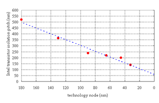
In semiconductor technology, copper interconnects are used in silicon integrated circuits (ICs) to reduce propagation delays and power consumption. Since copper is a better conductor than aluminium, ICs using copper for their interconnects can have interconnects with narrower dimensions, and use less energy to pass electricity through them. Together, these effects lead to ICs with better performance. They were first introduced by IBM, with assistance from Motorola, in 1997.

Deep reactive-ion etching (DRIE) is a highly anisotropic etch process used to create deep penetration, steep-sided holes and trenches in wafers/substrates, typically with high aspect ratios. It was developed for microelectromechanical systems (MEMS), which require these features, but is also used to excavate trenches for high-density capacitors for DRAM and more recently for creating through silicon vias (TSVs) in advanced 3D wafer level packaging technology.

Surface finishing is a broad range of industrial processes that alter the surface of a manufactured item to achieve a certain property. Finishing processes may be employed to: improve appearance, adhesion or wettability, solderability, corrosion resistance, tarnish resistance, chemical resistance, wear resistance, hardness, modify electrical conductivity, remove burrs and other surface flaws, and control the surface friction. In limited cases some of these techniques can be used to restore original dimensions to salvage or repair an item. An unfinished surface is often called mill finish.

Front end of line

The front-end-of-line (FEOL) is the first portion of IC fabrication where the individual devices are patterned in the semiconductor. FEOL generally covers everything up to the deposition of metal interconnect layers.

Microfabrication processes of fabrication of miniature structures

Microfabrication is the process of fabricating miniature structures of micrometre scales and smaller. Historically, the earliest microfabrication processes were used for integrated circuit fabrication, also known as "semiconductor manufacturing" or "semiconductor device fabrication". In the last two decades microelectromechanical systems (MEMS), microsystems, micromachines and their subfields, microfluidics/lab-on-a-chip, optical MEMS, RF MEMS, PowerMEMS, BioMEMS and their extension into nanoscale have re-used, adapted or extended microfabrication methods. Flat-panel displays and solar cells are also using similar techniques.

Etching (microfabrication) technique in microfabrication

Etching is used in microfabrication to chemically remove layers from the surface of a wafer during manufacturing. Etching is a critically important process module, and every wafer undergoes many etching steps before it is complete.

LOCOS, short for LOCal Oxidation of Silicon, is a microfabrication process where silicon dioxide is formed in selected areas on a silicon wafer having the Si-SiO2 interface at a lower point than the rest of the silicon surface.

Ultrasonic machining

Ultrasonic machining, or strictly speaking the "Ultrasonic vibration machining", is a subtraction manufacturing process that removes material from the surface of a part through high frequency, low amplitude vibrations of a tool against the material surface in the presence of fine abrasive particles. The tool travels vertically or orthogonal to the surface of the part at amplitudes of 0.05 to 0.125 mm. The fine abrasive grains are mixed with water to form a slurry that is distributed across the part and the tip of the tool. Typical grain sizes of the abrasive material range from 100 to 1000, where smaller grains produce smoother surface finishes.

Eco pickled surface (EPS) is a process applied to hot rolled sheet steel to remove all surface oxides and clean the steel surface. Steel which has undergone the EPS process acquires a high degree of resistance to subsequent development of surface oxide (rust), so long as it does not come into direct contact with moisture. EPS was developed by The Material Works, Ltd., which has filed several patent applications covering the process. It is primarily intended to be a replacement of the familiar acid pickling process wherein steel strip is immersed in solutions of hydrochloric and sulfuric acids to chemically remove oxides.

Thermocompression bonding describes a wafer bonding technique and is also referred to as diffusion bonding, pressure joining, thermocompression welding or solid-state welding. Two metals, e.g. gold (Au)-gold (Au), are brought into atomic contact applying force and heat simultaneously. The diffusion requires atomic contact between the surfaces due to the atomic motion. The atoms migrate from one crystal lattice to the other one based on crystal lattice vibration. This atomic interaction sticks the interface together. The diffusion process is described by the following three processes:

Direct bonding, or fusion bonding, describes a wafer bonding process without any additional intermediate layers. The bonding process is based on chemical bonds between two surfaces of any material possible meeting numerous requirements. These requirements are specified for the wafer surface as sufficiently clean, flat and smooth. Otherwise unbonded areas so called voids, i.e. interface bubbles, can occur.

Anodic bonding is a wafer bonding process to seal glass to either silicon or metal without introducing an intermediate layer; it is commonly used to seal glass to silicon wafers in electronics and microfluidics. This bonding technique, also known as field assisted bonding or electrostatic sealing, is mostly used for connecting silicon/glass and metal/glass through electric fields. The requirements for anodic bonding are clean and even wafer surfaces and atomic contact between the bonding substrates through a sufficiently powerful electrostatic field. Also necessary is the use of borosilicate glass containing a high concentration of alkali ions. The coefficient of thermal expansion (CTE) of the processed glass needs to be similar to those of the bonding partner.

Plasma-activated bonding is a derivative, directed to lower processing temperatures for direct bonding with hydrophilic surfaces. The main requirements for lowering temperatures of direct bonding are the use of materials melting at low temperatures and with different coefficients of thermal expansion (CTE).

Eutectic bonding

Eutectic bonding, also referred to as eutectic soldering, describes a wafer bonding technique with an intermediate metal layer that can produce a eutectic system. Those eutectic metals are alloys that transform directly from solid to liquid state, or vice versa from liquid to solid state, at a specific composition and temperature without passing a two-phase equilibrium, i.e. liquid and solid state. The fact that the eutectic temperature can be much lower than the melting temperature of the two or more pure elements can be important in eutectic bonding.

Glass frit bonding, also referred to as glass soldering or seal glass bonding, describes a wafer bonding technique with an intermediate glass layer. It is a widely used encapsulation technology for surface micro-machined structures, e.g., accelerometers or gyroscopes. This technique utilizes low melting glass and therefore provides various advantages including that viscosity of glass decreases with an increase of temperature. The viscous flow of glass has effects to compensate and planarize surface irregularities, convenient for bonding wafers with a high roughness due to plasma etching or deposition. A low viscosity promotes hermetically sealed encapsulation of structures based on a better adaption of the structured shapes. Further, the coefficient of thermal expansion (CTE) of the glass material is adapted to silicon. This results in low stress in the bonded wafer pair.

Chemistry of photolithography

Photolithography is a process in removing select portions of thin films used in microfabrication. Microfabrication is the production of parts on the micro- and nano- scale, typically on the surface of silicon wafers for the production of microelectromechanical systems (MEMS). Photolithography makes this process possible through the combined use of hexamethyldisilazane (HMDS), photoresist, a spin or spray coater, photomask, an exposure system and other various chemicals. By carefully manipulating these factors it is possible to create nearly any geometry microstructure on the surface of a silicon wafer. The chemical interaction between all the different components and the surface of the silicon wafer makes photolithography an interesting chemistry problem. Current science has been able to create features on the surface of silicon wafers between 1 and 100 µm.

In integrated circuits (ICs), interconnects are structures that connect two or more circuit elements together electrically. The design and layout of interconnects on an IC is vital to its proper function, performance, power efficiency, reliability, and fabrication yield. The material interconnects are made from depends on many factors. Chemical and mechanical compatibility with the semiconductor substrate, and the dielectric in between the levels of interconnect is necessary, otherwise barrier layers are needed. Suitability for fabrication is also required; some chemistries and processes prevent integration of materials and unit processes into a larger technology (recipe) for IC fabrication. In fabrication, interconnects are formed during the back-end-of-line after the fabrication of the transistors on the substrate.

References

  1. Mahadevaiyer Krishnan, Jakub W. Nalaskowsk, and Lee M. Cook, "Chemical Mechanical Planarization: Slurry Chemistry, Materials, and Mechanisms" Chem. Rev., 2010, vol. 110, pp 178–204. doi : 10.1021/cr900170z
  2. Awano,Y.: (2006), "Carbon Nanotube (CNT) Via Interconnect Technologies: Low temperature CVD growth and chemical mechanical planarization for vertically aligned CNTs". Proc. 2006 ICPT, 10

Books