Fabrication may refer to:
Contents
- Manufacturing, specifically the crafting of individual parts as a solo product or as part of a larger combined product.
Fabrication may refer to:

An integrated circuit or monolithic integrated circuit is a set of electronic circuits on one small flat piece of semiconductor material, usually silicon. Large numbers of tiny MOSFETs integrate into a small chip. This results in circuits that are orders of magnitude smaller, faster, and less expensive than those constructed of discrete electronic components. The IC's mass production capability, reliability, and building-block approach to integrated circuit design has ensured the rapid adoption of standardized ICs in place of designs using discrete transistors. ICs are now used in virtually all electronic equipment and have revolutionized the world of electronics. Computers, mobile phones and other home appliances are now inextricable parts of the structure of modern societies, made possible by the small size and low cost of ICs such as modern computer processors and microcontrollers.

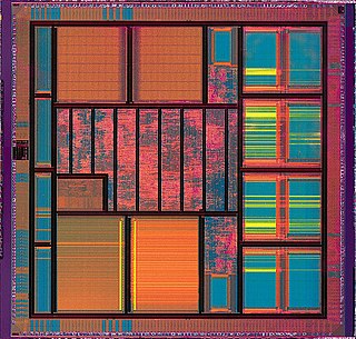
Semiconductor device fabrication is the process used to manufacture semiconductor devices, typically integrated circuit (IC) chips such as modern computer processors, microcontrollers, and memory chips such as NAND flash and DRAM that are present in everyday electrical and electronic devices. It is a multiple-step sequence of photolithographic and chemical processing steps during which electronic circuits are gradually created on a wafer made of pure semiconducting material. Silicon is almost always used, but various compound semiconductors are used for specialized applications.
A semiconductor material has an electrical conductivity value falling between that of a conductor, such as metallic copper, and an insulator, such as glass. Its resistivity falls as its temperature rises; metals behave in the opposite way. Its conducting properties may be altered in useful ways by introducing impurities ("doping") into the crystal structure. When two differently doped regions exist in the same crystal, a semiconductor junction is created. The behavior of charge carriers, which include electrons, ions, and electron holes, at these junctions is the basis of diodes, transistors, and most modern electronics. Some examples of semiconductors are silicon, germanium, gallium arsenide, and elements near the so-called "metalloid staircase" on the periodic table. After silicon, gallium arsenide is the second-most common semiconductor and is used in laser diodes, solar cells, microwave-frequency integrated circuits, and others. Silicon is a critical element for fabricating most electronic circuits.
Very large-scale integration (VLSI) is the process of creating an integrated circuit (IC) by combining millions or billions of MOS transistors onto a single chip. VLSI began in the 1970s when MOS integrated circuit chips were widely adopted, enabling complex semiconductor and telecommunication technologies to be developed. The microprocessor and memory chips are VLSI devices. Before the introduction of VLSI technology, most ICs had a limited set of functions they could perform. An electronic circuit might consist of a CPU, ROM, RAM and other glue logic. VLSI enables IC designers to add all of these into one chip.

A semiconductor device is an electronic component that relies on the electronic properties of a semiconductor material for its function. Its conductivity lies between conductors and insulators. Semiconductor devices have replaced vacuum tubes in most applications. They conduct electric current in the solid state, rather than as free electrons across a vacuum or as free electrons and ions through an ionized gas.

The metal–oxide–semiconductor field-effect transistor is a type of field-effect transistor (FET), most commonly fabricated by the controlled oxidation of silicon. It has an insulated gate, the voltage of which determines the conductivity of the device. This ability to change conductivity with the amount of applied voltage can be used for amplifying or switching electronic signals. A metal-insulator-semiconductor field-effect transistor or MISFET is a term almost synonymous with MOSFET. Another synonym is IGFET for insulated-gate field-effect transistor.

EEPROM (also called E2PROM) stands for electrically erasable programmable read-only memory and is a type of non-volatile memory used in computers, integrated in microcontrollers for smart cards and remote keyless systems, and other electronic devices to store relatively small amounts of data by allowing individual bytes to be erased and reprogrammed.

An application-specific integrated circuit is an integrated circuit (IC) chip customized for a particular use, rather than intended for general-purpose use. For example, a chip designed to run in a digital voice recorder or a high-efficiency video codec is an ASIC. Application-specific standard product (ASSP) chips are intermediate between ASICs and industry standard integrated circuits like the 7400 series or the 4000 series. ASIC chips are typically fabricated using metal-oxide-semiconductor (MOS) technology, as MOS integrated circuit chips.
Bipolar CMOS (BiCMOS) is a semiconductor technology that integrates two semiconductor technologies, those of the bipolar junction transistor and the CMOS logic gate, into a single integrated circuit. In more recent times the bipolar processes have been extended to include high mobility devices using silicon–germanium junctions.
In semiconductor manufacturing, silicon on insulator (SOI) technology is fabrication of silicon semiconductor devices in a layered silicon–insulator–silicon substrate, to reduce parasitic capacitance within the device, thereby improving performance. SOI-based devices differ from conventional silicon-built devices in that the silicon junction is above an electrical insulator, typically silicon dioxide or sapphire. The choice of insulator depends largely on intended application, with sapphire being used for high-performance radio frequency (RF) and radiation-sensitive applications, and silicon dioxide for diminished short-channel effects in other microelectronics devices. The insulating layer and topmost silicon layer also vary widely with application.

Metal fabrication is the creation of metal structures by cutting, bending and assembling processes. It is a value-added process involving the creation of machines, parts, and structures from various raw materials.

Microfabrication is the process of fabricating miniature structures of micrometre scales and smaller. Historically, the earliest microfabrication processes were used for integrated circuit fabrication, also known as "semiconductor manufacturing" or "semiconductor device fabrication". In the last two decades microelectromechanical systems (MEMS), microsystems, micromachines and their subfields, microfluidics/lab-on-a-chip, optical MEMS, RF MEMS, PowerMEMS, BioMEMS and their extension into nanoscale have re-used, adapted or extended microfabrication methods. Flat-panel displays and solar cells are also using similar techniques.
A hybrid silicon laser is a semiconductor laser fabricated from both silicon and group III-V semiconductor materials. The hybrid silicon laser was developed to address the lack of a silicon laser to enable fabrication of low-cost, mass-producible silicon optical devices. The hybrid approach takes advantage of the light-emitting properties of III-V semiconductor materials combined with the process maturity of silicon to fabricate electrically driven lasers on a silicon wafer that can be integrated with other silicon photonic devices.
In semiconductor electronics fabrication technology, a self-aligned gate is a transistor manufacturing feature whereby the gate electrode of a MOSFET is used as a mask for the doping of the source and drain regions. This technique ensures that the gate is naturally and precisely aligned to the edges of the source and drain.
The term die shrink refers to the scaling of metal-oxide-semiconductor (MOS) devices. The act of shrinking a die is to create a somewhat identical circuit using a more advanced fabrication process, usually involving an advance of lithographic nodes. This reduces overall costs for a chip company, as the absence of major architectural changes to the processor lowers research and development costs, while at the same time allowing more processor dies to be manufactured on the same piece of silicon wafer, resulting in less cost per product sold.
A semiconductor package is a metal, plastic, glass, or ceramic casing containing one or more discrete semiconductor devices or integrated circuits. Individual components are fabricated on semiconductor wafers before being diced into die, tested, and packaged. The package provides a means for connecting it to the external environment, such as printed circuit board, via leads such as lands, balls, or pins; and protection against threats such as mechanical impact, chemical contamination, and light exposure. Additionally, it helps dissipate heat produced by the device, with or without the aid of a heat spreader. There are thousands of package types in use. Some are defined by international, national, or industry standards, while others are particular to an individual manufacturer.
Stanley Shanfield serves as a Distinguished Member of the Technical Staff and Technical Director of Advanced Hardware Development at the Charles Stark Draper Laboratory in Cambridge, Massachusetts, a post he has held since 2003. He is the holder of seven patents and has led teams responsible for inventing and manufacturing new technologies in the fields of semiconductor device fabrication and optical electronics.

Dawon Kahng was a Korean-American electrical engineer and inventor, known for his work in solid-state electronics. He is best known for inventing the MOSFET, along with his colleague Mohamed Atalla, in 1959. Kahng and Atalla developed both the PMOS and NMOS processes for MOSFET semiconductor device fabrication. The MOSFET is the most widely used type of transistor, and the basic element in most modern electronic equipment.
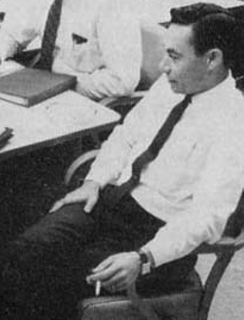
Mohamed M. Atalla was an Egyptian-American engineer, physicist, cryptographer, inventor and entrepreneur. He was a semiconductor pioneer who made important contributions to modern electronics. He is best known for inventing the MOSFET in 1959, which along with Atalla's earlier surface passivation and thermal oxidation processes, revolutionized the electronics industry. He is also known as the founder of the data security company Atalla Corporation, founded in 1972. He received the Stuart Ballantine Medal and was inducted into the National Inventors Hall of Fame for his important contributions to semiconductor technology as well as data security.
Glossary of microelectronics manufacturing terms