A charge-coupled device (CCD) is an integrated circuit containing an array of linked, or coupled, capacitors. Under the control of an external circuit, each capacitor can transfer its electric charge to a neighboring capacitor. CCD sensors are a major technology used in digital imaging.
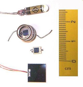
A photodiode is a semiconductor diode sensitive to photon radiation, such as visible light, infrared or ultraviolet radiation, X-rays and gamma rays. It produces an electrical current when it absorbs photons. This can be used for detection and measurement applications, or for the generation of electrical power in solar cells. Photodiodes are used in a wide range of applications throughout the electromagnetic spectrum from visible light photocells to gamma ray spectrometers.

Holography is a technique that enables a wavefront to be recorded and later reconstructed. It is best known as a method of generating three-dimensional images, and has a wide range of other uses, including data storage, microscopy, and interferometry. In principle, it is possible to make a hologram for any type of wave.

An optical mouse is a computer mouse which uses a light source, typically a light-emitting diode (LED), and a light detector, such as an array of photodiodes, to detect movement relative to a surface. Variations of the optical mouse have largely replaced the older mechanical mouse design, which uses moving parts to sense motion.

Photonics is a branch of optics that involves the application of generation, detection, and manipulation of light in the form of photons through emission, transmission, modulation, signal processing, switching, amplification, and sensing.

The vertical-cavity surface-emitting laser is a type of semiconductor laser diode with laser beam emission perpendicular from the top surface, contrary to conventional edge-emitting semiconductor lasers which emit from surfaces formed by cleaving the individual chip out of a wafer. VCSELs are used in various laser products, including computer mice, fiber-optic communications, laser printers, Face ID, and smartglasses.

An opto-isolator is an electronic component that transfers electrical signals between two isolated circuits by using light. Opto-isolators prevent high voltages from affecting the system receiving the signal. Commercially available opto-isolators withstand input-to-output voltages up to 10 kV and voltage transients with speeds up to 25 kV/μs.

A single-photon avalanche diode (SPAD), also called Geiger-mode avalanche photodiode is a solid-state photodetector within the same family as photodiodes and avalanche photodiodes (APDs), while also being fundamentally linked with basic diode behaviours. As with photodiodes and APDs, a SPAD is based around a semi-conductor p-n junction that can be illuminated with ionizing radiation such as gamma, x-rays, beta and alpha particles along with a wide portion of the electromagnetic spectrum from ultraviolet (UV) through the visible wavelengths and into the infrared (IR).

Photodetectors, also called photosensors, are sensors of light or other electromagnetic radiation. There are a wide variety of photodetectors which may be classified by mechanism of detection, such as photoelectric or photochemical effects, or by various performance metrics, such as spectral response. Semiconductor-based photodetectors typically use a p–n junction that converts photons into charge. The absorbed photons make electron–hole pairs in the depletion region. Photodiodes and photo transistors are a few examples of photo detectors. Solar cells convert some of the light energy absorbed into electrical energy.

An electronic component is any basic discrete electronic device or physical entity part of an electronic system used to affect electrons or their associated fields. Electronic components are mostly industrial products, available in a singular form and are not to be confused with electrical elements, which are conceptual abstractions representing idealized electronic components and elements. A datasheet for an electronic component is a technical document that provides detailed information about the component's specifications, characteristics, and performance. Discrete circuits are made of individual electronic components that only perform one function each as packaged, which are known as discrete components, although strictly the term discrete component refers to such a component with semiconductor material such as individual transistors.
An image sensor or imager is a sensor that detects and conveys information used to form an image. It does so by converting the variable attenuation of light waves into signals, small bursts of current that convey the information. The waves can be light or other electromagnetic radiation. Image sensors are used in electronic imaging devices of both analog and digital types, which include digital cameras, camera modules, camera phones, optical mouse devices, medical imaging equipment, night vision equipment such as thermal imaging devices, radar, sonar, and others. As technology changes, electronic and digital imaging tends to replace chemical and analog imaging.
An active-pixel sensor (APS) is an image sensor, which was invented by Peter J.W. Noble in 1968, where each pixel sensor unit cell has a photodetector and one or more active transistors. In a metal–oxide–semiconductor (MOS) active-pixel sensor, MOS field-effect transistors (MOSFETs) are used as amplifiers. There are different types of APS, including the early NMOS APS and the now much more common complementary MOS (CMOS) APS, also known as the CMOS sensor. CMOS sensors are used in digital camera technologies such as cell phone cameras, web cameras, most modern digital pocket cameras, most digital single-lens reflex cameras (DSLRs), mirrorless interchangeable-lens cameras (MILCs), and lensless imaging for, e.g., blood cells.
A holographic display is a type of 3D display that utilizes light diffraction to display a three-dimensional image to the viewer. Holographic displays are distinguished from other forms of 3D displays in that they do not require the viewer to wear any special glasses or use external equipment to be able to see the image, and do not cause a vergence-accommodation conflict.
A structured-light 3D scanner is a device that measures the three-dimensional shape of an object by projecting light patterns—such as grids or stripes—onto it and capturing their deformation with cameras. This technique allows for precise surface reconstruction by analyzing the displacement of the projected patterns, which are processed into detailed 3D models using specialized algorithms.

A time-of-flight camera, also known as time-of-flight sensor, is a range imaging camera system for measuring distances between the camera and the subject for each point of the image based on time-of-flight, the round trip time of an artificial light signal, as provided by a laser or an LED. Laser-based time-of-flight cameras are part of a broader class of scannerless LIDAR, in which the entire scene is captured with each laser pulse, as opposed to point-by-point with a laser beam such as in scanning LIDAR systems. Time-of-flight camera products for civil applications began to emerge around 2000, as the semiconductor processes allowed the production of components fast enough for such devices. The systems cover ranges of a few centimeters up to several kilometers.
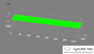
Digital holographic microscopy (DHM) is digital holography applied to microscopy. Digital holographic microscopy distinguishes itself from other microscopy methods by not recording the projected image of the object. Instead, the light wave front information originating from the object is digitally recorded as a hologram, from which a computer calculates the object image by using a numerical reconstruction algorithm. The image forming lens in traditional microscopy is thus replaced by a computer algorithm. Other closely related microscopy methods to digital holographic microscopy are interferometric microscopy, optical coherence tomography and diffraction phase microscopy. Common to all methods is the use of a reference wave front to obtain amplitude (intensity) and phase information. The information is recorded on a digital image sensor or by a photodetector from which an image of the object is created (reconstructed) by a computer. In traditional microscopy, which do not use a reference wave front, only intensity information is recorded and essential information about the object is lost.
Sensors for arc welding are devices which – as a part of a fully mechanised welding equipment – are capable to acquire information about position and, if possible, about the geometry of the intended weld at the workpiece and to provide respective data in a suitable form for the control of the weld torch position and, if possible, for the arc welding process parameters.
James Robert Biard was an American electrical engineer and inventor who held 73 U.S. patents. Some of his more significant patents include the first infrared light-emitting diode (LED), the optical isolator, Schottky clamped logic circuits, silicon Metal Oxide Semiconductor Read Only Memory, a low bulk leakage current avalanche photodetector, and fiber-optic data links. In 1980, Biard became a member of the staff of Texas A&M University as an adjunct professor of electrical engineering. In 1991, he was elected as a member into the National Academy of Engineering for contributions to semiconductor light-emitting diodes and lasers, Schottky-clamped logic, and read-only memories.
