Related Research Articles
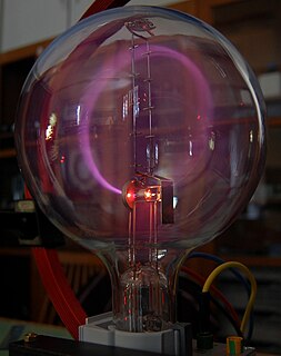
Cathode rays are streams of electrons observed in discharge tubes. If an evacuated glass tube is equipped with two electrodes and a voltage is applied, glass behind the positive electrode is observed to glow, due to electrons emitted from the cathode. They were first observed in 1869 by German physicist Julius PlüKathodenstrahlen, or cathode rays. In 1897, British physicist J. J. Thomson showed that cathode rays were composed of a previously unknown negatively charged particle, which was later named the electron. Cathode-ray tubes (CRTs) use a focused beam of electrons deflected by electric or magnetic fields to render an image on a screen.
In integrated circuit manufacturing, photolithography or optical lithography is a general term for techniques that use light to produce minutely patterned thin films of suitable materials over a substrate, such as a silicon wafer, to protect selected areas of it during subsequent etching, deposition, or implantation operations. Typically, ultraviolet light is used to transfer a geometric design from an optical mask to a light-sensitive chemical (photoresist) coated on the substrate. The photoresist either breaks down or hardens where it is exposed to light. The patterned film is the created by removing the softer parts of the coating with appropriate solvents.
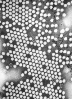
Transmission electron microscopy (TEM) is a microscopy technique in which a beam of electrons is transmitted through a specimen to form an image. The specimen is most often an ultrathin section less than 100 nm thick or a suspension on a grid. An image is formed from the interaction of the electrons with the sample as the beam is transmitted through the specimen. The image is then magnified and focused onto an imaging device, such as a fluorescent screen, a layer of photographic film, or a sensor such as a scintillator attached to a charge-coupled device.
Reflection high-energy electron diffraction (RHEED) is a technique used to characterize the surface of crystalline materials. RHEED systems gather information only from the surface layer of the sample, which distinguishes RHEED from other materials characterization methods that also rely on diffraction of high-energy electrons. Transmission electron microscopy, another common electron diffraction method samples the bulk of the sample due to the geometry of the system. Low-energy electron diffraction (LEED) is also surface sensitive, but LEED achieves surface sensitivity through the use of low energy electrons.
Electron-beam lithography is the practice of scanning a focused beam of electrons to draw custom shapes on a surface covered with an electron-sensitive film called a resist (exposing). The electron beam changes the solubility of the resist, enabling selective removal of either the exposed or non-exposed regions of the resist by immersing it in a solvent (developing). The purpose, as with photolithography, is to create very small structures in the resist that can subsequently be transferred to the substrate material, often by etching.
A microprobe is an instrument that applies a stable and well-focused beam of charged particles to a sample.
A particle-beam weapon uses a high-energy beam of atomic or subatomic particles to damage the target by disrupting its atomic and/or molecular structure. A particle-beam weapon is a type of directed-energy weapon, which directs energy in a particular and focused direction using particles with minuscule mass. Some particle-beam weapons have potential practical applications, e.g. as an antiballistic missile defense system for the United States and its cancelled Strategic Defense Initiative. They have been known by myriad names: phasers, disruptors, particle accelerator guns, ion cannons, proton beams, lightning rays, rayguns, etc.
Nanolithography (NL) is a growing field of techniques within nanotechnology dealing with the engineering of nanometer-scale structures on various materials.

ALICE is one of eight detector experiments at the Large Hadron Collider at CERN. The other seven are: ATLAS, CMS, TOTEM, LHCb, LHCf, MoEDAL and FASER.

Focused ion beam, also known as FIB, is a technique used particularly in the semiconductor industry, materials science and increasingly in the biological field for site-specific analysis, deposition, and ablation of materials. A FIB setup is a scientific instrument that resembles a scanning electron microscope (SEM). However, while the SEM uses a focused beam of electrons to image the sample in the chamber, a FIB setup uses a focused beam of ions instead. FIB can also be incorporated in a system with both electron and ion beam columns, allowing the same feature to be investigated using either of the beams. FIB should not be confused with using a beam of focused ions for direct write lithography. These are generally quite different systems where the material is modified by other mechanisms.
X-ray optics is the branch of optics that manipulates X-rays instead of visible light. It deals with focusing and other ways of manipulating the X-ray beams for research techniques such as X-ray crystallography, X-ray fluorescence, small-angle X-ray scattering, X-ray microscopy, X-ray phase-contrast imaging, X-ray astronomy etc.
Interference lithography is a technique for patterning regular arrays of fine features, without the use of complex optical systems or photomasks.

Channelling is the process that constrains the path of a charged particle in a crystalline solid.
Helium atom scattering (HAS) is a surface analysis technique used in materials science. HAS provides information about the surface structure and lattice dynamics of a material by measuring the diffracted atoms from a monochromatic helium beam incident on the sample.

Low-energy ion scattering spectroscopy (LEIS), sometimes referred to simply as ion scattering spectroscopy (ISS), is a surface-sensitive analytical technique used to characterize the chemical and structural makeup of materials. LEIS involves directing a stream of charged particles known as ions at a surface and making observations of the positions, velocities, and energies of the ions that have interacted with the surface. Data that is thus collected can be used to deduce information about the material such as the relative positions of atoms in a surface lattice and the elemental identity of those atoms. LEIS is closely related to both medium-energy ion scattering (MEIS) and high-energy ion scattering, differing primarily in the energy range of the ion beam used to probe the surface. While much of the information collected using LEIS can be obtained using other surface science techniques, LEIS is unique in its sensitivity to both structure and composition of surfaces. Additionally, LEIS is one of a very few surface-sensitive techniques capable of directly observing hydrogen atoms, an aspect that may make it an increasingly more important technique as the hydrogen economy is being explored.
Proton beam writing is a direct-write lithography process that uses a focused beam of high energy (MeV) protons to pattern resist material at nanodimensions. The process, although similar in many ways to direct writing using electrons, nevertheless offers some interesting and unique advantages.

X-ray lithography, is a process used in electronic industry to selectively remove parts of a thin film. It uses X-rays to transfer a geometric pattern from a mask to a light-sensitive chemical photoresist, or simply "resist," on the substrate. A series of chemical treatments then engraves the produced pattern into the material underneath the photoresist.

A spectrometer is a scientific instrument used to separate and measure spectral components of a physical phenomenon. Spectrometer is a broad term often used to describe instruments that measure a continuous variable of a phenomenon where the spectral components are somehow mixed. In visible light a spectrometer can separate white light and measure individual narrow bands of color, called a spectrum. A mass spectrometer measures the spectrum of the masses of the atoms or molecules present in a gas. The first spectrometers were used to split light into an array of separate colors. Spectrometers were developed in early studies of physics, astronomy, and chemistry. The capability of spectroscopy to determine chemical composition drove its advancement and continues to be one of its primary uses. Spectrometers are used in astronomy to analyze the chemical composition of stars and planets, and spectrometers gather data on the origin of the universe.

The scanning helium microscope (SHeM) is a novel form of microscopy that uses low energy neutral helium atoms to image the surface of a sample without any damage to the sample caused by the imaging process. Since helium is inert and neutral, it can be used to study delicate and insulating surfaces. Images are formed by rastering a sample underneath an atom beam and monitoring the flux of atoms that are scattered into a detector at each point.
References
- ↑ F. Watt∗, A. A. Bettiol, J. A. Van Kan, E. J. Teo and M. B. H. Breese http://www.ciba.nus.edu.sg/publications/files/pbw/pbw2005_1.pdf Archived 2011-07-21 at the Wayback Machine "Ion Beam Lithography and Nanofabrication: a Review"], The Guardian , London, 17 December 2004. Retrieved on 2011-03-03.
- ↑ Dhara Parikh, Barry Craver, Hatem N. Nounu, Fu-On Fong, and John C. Wolfe, "Nanoscale Pattern Definition on Nonplanar Surfaces Using Ion Beam Proximity Lithography and Conformal Plasma-Deposited Resist", Journal of microelectromechanical systems, vol. 17, no. 3, June 2008
- ↑ Madou, Mark (2012). Fundamentals of Microfabrication and Nanotechnology volume 2. Boca Raton, Fl: CRC Press. p. 655. ISBN 978-1-4200-5519-1.