
The photoelectric effect is the emission of electrons from a material caused by electromagnetic radiation (light). Electrons emitted in this manner are called photoelectrons. The phenomenon is studied in condensed matter physics, solid state, and quantum chemistry to draw inferences about the properties of atoms, molecules and solids. The effect has found use in electronic devices specialized for light detection and precisely timed electron emission.

An electron and an electron hole that are attracted to each other by the Coulomb force can form a bound state called an exciton. It is an electrically neutral quasiparticle that exists mainly in condensed matter, including insulators, semiconductors, some metals, but also in certain atoms, molecules and liquids. The exciton is regarded as an elementary excitation that can transport energy without transporting net electric charge.
In solid-state physics, the work function is the minimum thermodynamic work needed to remove an electron from a solid to a point in the vacuum immediately outside the solid surface. Here "immediately" means that the final electron position is far from the surface on the atomic scale, but still too close to the solid to be influenced by ambient electric fields in the vacuum. The work function is not a characteristic of a bulk material, but rather a property of the surface of the material.

Photoluminescence is light emission from any form of matter after the absorption of photons. It is one of many forms of luminescence and is initiated by photoexcitation, hence the prefix photo-. Following excitation, various relaxation processes typically occur in which other photons are re-radiated. Time periods between absorption and emission may vary: ranging from short femtosecond-regime for emission involving free-carrier plasma in inorganic semiconductors up to milliseconds for phosphoresence processes in molecular systems; and under special circumstances delay of emission may even span to minutes or hours.

Optoelectronics is the study and application of electronic devices and systems that find, detect and control light, usually considered a sub-field of photonics. In this context, light often includes invisible forms of radiation such as gamma rays, X-rays, ultraviolet and infrared, in addition to visible light. Optoelectronic devices are electrical-to-optical or optical-to-electrical transducers, or instruments that use such devices in their operation.

A scintillator is a material that exhibits scintillation, the property of luminescence, when excited by ionizing radiation. Luminescent materials, when struck by an incoming particle, absorb its energy and scintillate. Sometimes, the excited state is metastable, so the relaxation back down from the excited state to lower states is delayed. The process then corresponds to one of two phenomena: delayed fluorescence or phosphorescence. The correspondence depends on the type of transition and hence the wavelength of the emitted optical photon.

A photocathode is a surface engineered to convert light (photons) into electrons using the photoelectric effect. Photocathodes are important in accelerator physics where they are utilised in a photoinjector to generate high brightness electron beams. Electron beams generated with photocathodes are commonly used for free electron lasers and for ultrafast electron diffraction. Photocathodes are also commonly used as the negatively charged electrode in a light detection device such as a photomultiplier, phototube and image intensifier.

An F center or Farbe center is a type of crystallographic defect in which an anionic vacancy in a crystal lattice is occupied by one or more unpaired electrons. Electrons in such a vacancy in a crystal lattice tend to absorb light in the visible spectrum such that a material that is usually transparent becomes colored. The greater the number of F centers, the more intense the color of the compound. F centers are a type of color center.
Photoemission spectroscopy (PES), also known as photoelectron spectroscopy, refers to energy measurement of electrons emitted from solids, gases or liquids by the photoelectric effect, in order to determine the binding energies of electrons in the substance. The term refers to various techniques, depending on whether the ionization energy is provided by X-ray, XUV or UV photons. Regardless of the incident photon beam, however, all photoelectron spectroscopy revolves around the general theme of surface analysis by measuring the ejected electrons.
Photoemission electron microscopy is a type of electron microscopy that utilizes local variations in electron emission to generate image contrast. The excitation is usually produced by ultraviolet light, synchrotron radiation or X-ray sources. PEEM measures the coefficient indirectly by collecting the emitted secondary electrons generated in the electron cascade that follows the creation of the primary core hole in the absorption process. PEEM is a surface sensitive technique because the emitted electrons originate from a shallow layer. In physics, this technique is referred to as PEEM, which goes together naturally with low-energy electron diffraction (LEED), and low-energy electron microscopy (LEEM). In biology, it is called photoelectron microscopy (PEM), which fits with photoelectron spectroscopy (PES), transmission electron microscopy (TEM), and scanning electron microscopy (SEM).
Organic semiconductors are solids whose building blocks are pi-bonded molecules or polymers made up by carbon and hydrogen atoms and – at times – heteroatoms such as nitrogen, sulfur and oxygen. They exist in the form of molecular crystals or amorphous thin films. In general, they are electrical insulators, but become semiconducting when charges are either injected from appropriate electrodes, upon doping or by photoexcitation.

Extreme ultraviolet radiation or high-energy ultraviolet radiation is electromagnetic radiation in the part of the electromagnetic spectrum spanning wavelengths shorter that the hydrogen Lyman-alpha line from 121 nm down to the X-ray band of 10 nm. By the Planck–Einstein equation the EUV photons have energies from 10.26 eV up to 124.24 eV where we enter the X-ray energies. EUV is naturally generated by the solar corona and artificially by plasma, high harmonic generation sources and synchrotron light sources. Since UVC extends to 100 nm, there is some overlap in the terms.
X-ray absorption near edge structure (XANES), also known as near edge X-ray absorption fine structure (NEXAFS), is a type of absorption spectroscopy that indicates the features in the X-ray absorption spectra (XAS) of condensed matter due to the photoabsorption cross section for electronic transitions from an atomic core level to final states in the energy region of 50–100 eV above the selected atomic core level ionization energy, where the wavelength of the photoelectron is larger than the interatomic distance between the absorbing atom and its first neighbour atoms.

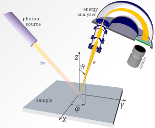
Angle-resolved photoemission spectroscopy (ARPES) is an experimental technique used in condensed matter physics to probe the allowed energies and momenta of the electrons in a material, usually a crystalline solid. It is based on the photoelectric effect, in which an incoming photon of sufficient energy ejects an electron from the surface of a material. By directly measuring the kinetic energy and emission angle distributions of the emitted photoelectrons, the technique can map the electronic band structure and Fermi surfaces. ARPES is best suited for the study of one- or two-dimensional materials. It has been used by physicists to investigate high-temperature superconductors, graphene, topological materials, quantum well states, and materials exhibiting charge density waves.
Ultraviolet photoelectron spectroscopy (UPS) refers to the measurement of kinetic energy spectra of photoelectrons emitted by molecules which have absorbed ultraviolet photons, in order to determine molecular orbital energies in the valence region.
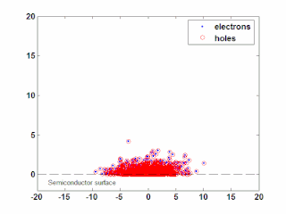
In semiconductor physics, the photo–Dember effect is the formation of a charge dipole in the vicinity of a semiconductor surface after ultra-fast photo-generation of charge carriers. The dipole forms owing to the difference of mobilities for holes and electrons which combined with the break of symmetry provided by the surface lead to an effective charge separation in the direction perpendicular to the surface. In an isolated sample, where the macroscopic flow of an electric current is prohibited, the fast carriers are slowed and the slow carriers are accelerated by an electric field, called the Dember field.
Laser-based angle-resolved photoemission spectroscopy is a form of angle-resolved photoemission spectroscopy that uses a laser as the light source. Photoemission spectroscopy is a powerful and sensitive experimental technique to study surface physics. It is based on the photoelectric effect originally observed by Heinrich Hertz in 1887 and later explained by Albert Einstein in 1905 that when a material is shone by light, the electrons can absorb photons and escape from the material with the kinetic energy: , where is the incident photon energy, the work function of the material. Since the kinetic energy of ejected electrons are highly associated with the internal electronic structure, by analyzing the photoelectron spectroscopy one can realize the fundamental physical and chemical properties of the material, such as the type and arrangement of local bonding, electronic structure and chemical composition.
Photoelectrochemical processes are processes in photoelectrochemistry; they usually involve transforming light into other forms of energy. These processes apply to photochemistry, optically pumped lasers, sensitized solar cells, luminescence, and photochromism.
A trion is a bound state of three charged particles. A negatively charged trion in crystals consists of two electrons and one hole, while a positively charged trion consists of two holes and one electron. The binding energy of a trion is largely determined by the exchange interaction between the two electrons (holes). The ground state of a negatively charged trion is a singlet. The triplet state is unbound in the absence of an additional potential or sufficiently strong magnetic field.
Paul Leon Hartman was an American experimental physicist, known for making pioneering measurements of synchrotron radiation.
