Related Research Articles
In computing, Streaming SIMD Extensions (SSE) is a single instruction, multiple data (SIMD) instruction set extension to the x86 architecture, designed by Intel and introduced in 1999 in their Pentium III series of central processing units (CPUs) shortly after the appearance of Advanced Micro Devices (AMD's) 3DNow!. SSE contains 70 new instructions, most of which work on single precision floating-point data. SIMD instructions can greatly increase performance when exactly the same operations are to be performed on multiple data objects. Typical applications are digital signal processing and graphics processing.
Visual Instruction Set, or VIS, is a SIMD instruction set extension for SPARC V9 microprocessors developed by Sun Microsystems. There are five versions of VIS: VIS 1, VIS 2, VIS 2+, VIS 3 and VIS 4.
The Athlon 64 is a ninth-generation, AMD64-architecture microprocessor produced by Advanced Micro Devices (AMD), released on September 23, 2003. It is the third processor to bear the name Athlon, and the immediate successor to the Athlon XP. The Athlon 64 was the second processor to implement the AMD64 architecture and the first 64-bit processor targeted at the average consumer. Variants of the Athlon 64 have been produced for Socket 754, Socket 939, Socket 940, and Socket AM2. It was AMD's primary consumer CPU, and primarily competed with Intel's Pentium 4, especially the Prescott and Cedar Mill core revisions.
SSE2 is one of the Intel SIMD processor supplementary instruction sets introduced by Intel with the initial version of the Pentium 4 in 2000. SSE2 instructions allow the use of XMM (SIMD) registers on x86 instruction set architecture processors. These registers can load up to 128 bits of data and perform instructions, such as vector addition and multiplication, simultaneously.
SSE3, Streaming SIMD Extensions 3, also known by its Intel code name Prescott New Instructions (PNI), is the third iteration of the SSE instruction set for the IA-32 (x86) architecture. Intel introduced SSE3 in early 2004 with the Prescott revision of their Pentium 4 CPU. In April 2005, AMD introduced a subset of SSE3 in revision E of their Athlon 64 CPUs. The earlier SIMD instruction sets on the x86 platform, from oldest to newest, are MMX, 3DNow!, SSE, and SSE2.
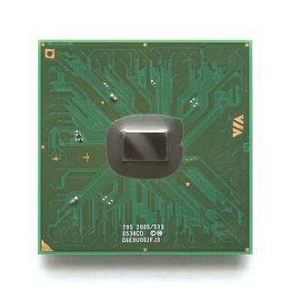
The VIA C7 is an x86 central processing unit designed by Centaur Technology and sold by VIA Technologies.
The AMD Family 10h, or K10, is a microprocessor microarchitecture by AMD based on the K8 microarchitecture. The first third-generation Opteron products for servers were launched on September 10, 2007, with the Phenom processors for desktops following and launching on November 11, 2007 as the immediate successors to the K8 series of processors.

The VIA Nano is a 64-bit CPU for personal computers. The VIA Nano was released by VIA Technologies in 2008 after five years of development by its CPU division, Centaur Technology. This new Isaiah 64-bit architecture was designed from scratch, unveiled on 24 January 2008, and launched on 29 May, including low-voltage variants and the Nano brand name. The processor supports a number of VIA-specific x86 extensions designed to boost efficiency in low-power appliances.
References
- ↑ "IA-32 implementation: VIA Cyrix III". sandpile.org. Archived from the original on 2007-07-09. Retrieved 2007-07-23.
- ↑ "IA-32 implementation: VIA C3". sandpile.org. Archived from the original on 2007-07-17. Retrieved 2007-07-23.
- ↑ "IA-32 implementation: VIA C7". sandpile.org. Archived from the original on 2007-06-30. Retrieved 2007-07-23.
- "VIA Nano X2 SPEC2000 ratio and rate scores". Via.com. Archived from the original on 7 February 2014. Retrieved 3 February 2014.
- ↑ "VIA QuadCore Processor". Via.com. Retrieved 2014-02-03.
- ↑ "VIA Nano X2 Whitepaper" (PDF). Via.com. Archived from the original (PDF) on 27 May 2012. Retrieved 3 February 2014.
- ↑ "VIA CenTaur Develops a Multi-core x86 Processor for Enterprise with in-built AI Hardware". TechPowerUp. November 18, 2019h. Retrieved 2020-07-28.
- ↑ "VIA CenTaur CHA NCORE AI CPU Pictured, a Socketed LGA Package". TechPowerUp. February 18, 2020. Retrieved 2020-07-28.
- ↑ "CHA - Microarchitectures - Centaur Technology - WikiChip". en.wikichip.org. Retrieved 2020-07-28.
- ↑ "The Last x86 Via Chip: Unreleased Next-Gen Centaur CNS Saved From Trash Bin, Tested". TomsHardware. 22 February 2022.
- ↑ "VIA x86 AI processor architecture, performance announcement: comparable to Intel 32 core". Small Tech News. December 11, 2019.
- ↑ "Centaur Releases In-Depth Analysis from The Linley Group for its NCORE-Equipped x86 Processor". TechPowerUp. December 9, 2019. Retrieved 2020-08-30.
- ↑ "World's First High-Performancex86 SoCwithIntegrated AI Coprocessor" (PDF). centtech. p. 4. Archived from the original on November 19, 2019.
{{cite web}}: CS1 maint: unfit URL (link)