Photolithography is a process used in the manufacturing of integrated circuits. It involves using light to transfer a pattern onto a substrate, typically a silicon wafer.
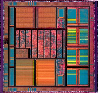
Very-large-scale integration (VLSI) is the process of creating an integrated circuit (IC) by combining millions or billions of MOS transistors onto a single chip. VLSI began in the 1970s when MOS integrated circuit chips were developed and then widely adopted, enabling complex semiconductor and telecommunications technologies. The microprocessor and memory chips are VLSI devices.

Taiwan Semiconductor Manufacturing Company Limited is a Taiwanese multinational semiconductor contract manufacturing and design company. It is the world's most valuable semiconductor company, the world's largest dedicated independent ("pure-play") semiconductor foundry, and Taiwan's largest company, with headquarters and main operations located in the Hsinchu Science Park in Hsinchu, Taiwan. Although the central government of Taiwan is the largest individual shareholder, the majority of TSMC is owned by foreign investors. In 2023, the company was ranked 44th in the Forbes Global 2000. Taiwan's exports of integrated circuits amounted to $184 billion in 2022, accounted for nearly 25 percent of Taiwan's GDP. TSMC constitutes about 30 percent of the Taiwan Stock Exchange's main index.
The semiconductor industry is the aggregate of companies engaged in the design and fabrication of semiconductors and semiconductor devices, such as transistors and integrated circuits. It's roots can be traced to the invention of the transistor by Shockley, Brattain, and Bardeen at Bell Labs in 1948. Bell Labs licensed the technology for $25,000, and soon many companies, including Motorola (1952), Schockley Semiconductor (1955), Sylvania, Centralab, Fairchild Semiconductor and Texas Instruments were making transistors. In 1958 Jack Kilby of Texas Instruments and Robert Noyce of Fairchild independently invented the Integrated Circuit, a method of producing multiple transistors on a single "chip" of Semiconductor material. This kicked off a number of rapid advances in fabrication technology leading to the exponential growth in semiconductor device production, known as Moore's law that has persisted over the past six or so decades. The industry's annual semiconductor sales revenue has since grown to over $481 billion, as of 2018.

A photomask is an opaque plate with transparent areas that allow light to shine through in a defined pattern. Photomasks are commonly used in photolithography for the production of integrated circuits to produce a pattern on a thin wafer of material. In semiconductor manufacturing, a mask is sometimes called a reticle.
The foundry model is a microelectronics engineering and manufacturing business model consisting of a semiconductor fabrication plant, or foundry, and an integrated circuit design operation, each belonging to separate companies or subsidiaries. It was first conceived by Morris Chang, the founder of the Taiwan Semiconductor Manufacturing Company Limited (TSMC).
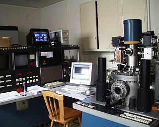
Electron-beam lithography is the practice of scanning a focused beam of electrons to draw custom shapes on a surface covered with an electron-sensitive film called a resist (exposing). The electron beam changes the solubility of the resist, enabling selective removal of either the exposed or non-exposed regions of the resist by immersing it in a solvent (developing). The purpose, as with photolithography, is to create very small structures in the resist that can subsequently be transferred to the substrate material, often by etching.

Extreme ultraviolet lithography is a technology used in the semiconductor industry for manufacturing integrated circuits (ICs). It is a type of photolithography that uses 13.5 nm extreme ultraviolet (EUV) light from a laser-pulsed tin (Sn) plasma to create intricate patterns on semiconductor substrates.

Phase-shift masks are photomasks that take advantage of the interference generated by phase differences to improve image resolution in photolithography. There exist alternating and attenuated phase shift masks. A phase-shift mask relies on the fact that light passing through a transparent media will undergo a phase change as a function of its optical thickness.

Optical proximity correction (OPC) is a photolithography enhancement technique commonly used to compensate for image errors due to diffraction or process effects. The need for OPC is seen mainly in the making of semiconductor devices and is due to the limitations of light to maintain the edge placement integrity of the original design, after processing, into the etched image on the silicon wafer. These projected images appear with irregularities such as line widths that are narrower or wider than designed, these are amenable to compensation by changing the pattern on the photomask used for imaging. Other distortions such as rounded corners are driven by the resolution of the optical imaging tool and are harder to compensate for. Such distortions, if not corrected for, may significantly alter the electrical properties of what was being fabricated. Optical proximity correction corrects these errors by moving edges or adding extra polygons to the pattern written on the photomask. This may be driven by pre-computed look-up tables based on width and spacing between features or by using compact models to dynamically simulate the final pattern and thereby drive the movement of edges, typically broken into sections, to find the best solution,. The objective is to reproduce the original layout drawn by the designer on the semiconductor wafer as well as possible.
The "32 nm" node is the step following the "45 nm" process in CMOS (MOSFET) semiconductor device fabrication. "32-nanometre" refers to the average half-pitch of a memory cell at this technology level.

Multiple patterning is a class of technologies for manufacturing integrated circuits (ICs), developed for photolithography to enhance the feature density. It is expected to be necessary for the 10 nm and 7 nm node semiconductor processes and beyond. The premise is that a single lithographic exposure may not be enough to provide sufficient resolution. Hence additional exposures would be needed, or else positioning patterns using etched feature sidewalls would be necessary.
The "14 nanometer process" refers to a marketing term for the MOSFET technology node that is the successor to the "22 nm" node. The "14 nm" was so named by the International Technology Roadmap for Semiconductors (ITRS). Until about 2011, the node following "22 nm" was expected to be "16 nm". All "14 nm" nodes use FinFET technology, a type of multi-gate MOSFET technology that is a non-planar evolution of planar silicon CMOS technology.
Computational lithography is the set of mathematical and algorithmic approaches designed to improve the resolution attainable through photolithography. Computational lithography came to the forefront of photolithography technologies in 2008 when the semiconductor industry faced challenges associated with the transition to a 22 nanometer CMOS microfabrication process and has become instrumental in further shrinking the design nodes and topology of semiconductor transistor manufacturing.
GlobalFoundries Inc. is a multinational semiconductor contract manufacturing and design company incorporated in the Cayman Islands and headquartered in Malta, New York. Created by the divestiture of the manufacturing arm of AMD, the company was privately owned by Mubadala Investment Company, a sovereign wealth fund of the United Arab Emirates, until an initial public offering (IPO) in October 2021.
Suss Microtec is a supplier of equipment and process solutions for the semiconductor, nano and microsystems technology and related markets with headquarters in Garching near Munich.
In semiconductor manufacturing, the International Roadmap for Devices and Systems defines the "5 nm" process as the MOSFET technology node following the "7 nm" node. In 2020, Samsung and TSMC entered volume production of "5 nm" chips, manufactured for companies including Apple, Huawei, Mediatek, Qualcomm and Marvell.
In semiconductor manufacturing, the "7 nm" process is a term for the MOSFET technology node following the "10 nm" node, defined by the International Roadmap for Devices and Systems (IRDS), which was preceded by the International Technology Roadmap for Semiconductors (ITRS). It is based on FinFET technology, a type of multi-gate MOSFET technology.
In the early twenty-first century; foreign investment, government regulations and incentives promoted growth in the Indian electronics industry. The semiconductor industry, which is its most important and resource-intensive sector, profited from the rapid growth in domestic demand. Many industries, including telecommunications, information technology, automotive, engineering, medical electronics, electricity and solar photovoltaic, defense and aerospace, consumer electronics, and appliances, required semiconductors. However, as of 2015, progress was threatened by the talent gap in the Indian sector, since 65 to 70 percent of the market was dependent on imports.
Multibeam is an American corporation that engages in the design, manufacture, and sale of semiconductor processing equipment used in the fabrication of integrated circuits. Headquartered in Santa Clara, in the Silicon Valley, Multibeam is led by Dr. David K. Lam, the founder and first CEO of Lam Research.