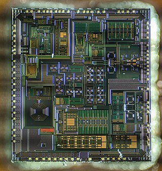
An integrated circuit (IC), also known as a microchip, computer chip, or simply chip, is a small electronic device made up of multiple interconnected electronic components such as transistors, resistors, and capacitors. These components are etched onto a small piece of semiconductor material, usually silicon. Integrated circuits are used in a wide range of electronic devices, including computers, smartphones, and televisions, to perform various functions such as processing and storing information. They have greatly impacted the field of electronics by enabling device miniaturization and enhanced functionality.

Semiconductor device fabrication is the process used to manufacture semiconductor devices, typically integrated circuits (ICs) such as computer processors, microcontrollers, and memory chips. It is a multiple-step photolithographic and physico-chemical process during which electronic circuits are gradually created on a wafer, typically made of pure single-crystal semiconducting material. Silicon is almost always used, but various compound semiconductors are used for specialized applications.

A transistor is a semiconductor device used to amplify or switch electrical signals and power. It is one of the basic building blocks of modern electronics. It is composed of semiconductor material, usually with at least three terminals for connection to an electronic circuit. A voltage or current applied to one pair of the transistor's terminals controls the current through another pair of terminals. Because the controlled (output) power can be higher than the controlling (input) power, a transistor can amplify a signal. Some transistors are packaged individually, but many more in miniature form are found embedded in integrated circuits. Because transistors are the key active components in practically all modern electronics, many people consider them one of the 20th century's greatest inventions.

A fin field-effect transistor (FinFET) is a multigate device, a MOSFET built on a substrate where the gate is placed on two, three, or four sides of the channel or wrapped around the channel, forming a double or even multi gate structure. These devices have been given the generic name "FinFETs" because the source/drain region forms fins on the silicon surface. The FinFET devices have significantly faster switching times and higher current density than planar CMOS technology.
Deep reactive-ion etching (DRIE) is a special subclass of reactive-ion etching (RIE). It enables highly anisotropic etch process used to create deep penetration, steep-sided holes and trenches in wafers/substrates, typically with high aspect ratios. It was developed for microelectromechanical systems (MEMS), which require these features, but is also used to excavate trenches for high-density capacitors for DRAM and more recently for creating through-silicon vias (TSVs) in advanced 3D wafer level packaging technology.

An active-pixel sensor (APS) is an image sensor, which was invented by Peter J.W. Noble in 1968, where each pixel sensor unit cell has a photodetector and one or more active transistors. In a metal–oxide–semiconductor (MOS) active-pixel sensor, MOS field-effect transistors (MOSFETs) are used as amplifiers. There are different types of APS, including the early NMOS APS and the now much more common complementary MOS (CMOS) APS, also known as the CMOS sensor. CMOS sensors are used in digital camera technologies such as cell phone cameras, web cameras, most modern digital pocket cameras, most digital single-lens reflex cameras (DSLRs), mirrorless interchangeable-lens cameras (MILCs), and lensless imaging for cells.
Nanoelectronics refers to the use of nanotechnology in electronic components. The term covers a diverse set of devices and materials, with the common characteristic that they are so small that inter-atomic interactions and quantum mechanical properties need to be studied extensively. Some of these candidates include: hybrid molecular/semiconductor electronics, one-dimensional nanotubes/nanowires or advanced molecular electronics.

A multigate device, multi-gate MOSFET or multi-gate field-effect transistor (MuGFET) refers to a metal–oxide–semiconductor field-effect transistor (MOSFET) that has more than one gate on a single transistor. The multiple gates may be controlled by a single gate electrode, wherein the multiple gate surfaces act electrically as a single gate, or by independent gate electrodes. A multigate device employing independent gate electrodes is sometimes called a multiple-independent-gate field-effect transistor (MIGFET). The most widely used multi-gate devices are the FinFET and the GAAFET, which are non-planar transistors, or 3D transistors.
Nanocircuits are electrical circuits operating on the nanometer scale where quantum mechanical effects become important. One nanometer is equal to 10−9 meters or a row of 10 hydrogen atoms. With such progressively smaller circuits, more can be fitted on a computer chip. This allows faster and more complex functions using less power. Nanocircuits are composed of three different fundamental components. These are transistors, interconnections, and architecture, all fabricated on the nanometer scale.
Chenming Calvin Hu is a Taiwanese-American electronic engineer who specializes in microelectronics. He is TSMC Distinguished Professor Emeritus in the electronic engineering and computer science department of the University of California, Berkeley, in the United States. In 2009, the Institute of Electrical and Electronics Engineers described him as a “microelectronics visionary … whose seminal work on metal-oxide semiconductor MOS reliability and device modeling has had enormous impact on the continued scaling of electronic devices”.
Mark S. Lundstrom is an American electrical engineering researcher, educator, and author. He is known for contributions to the theory, modeling, and understanding of semiconductor devices, especially nanoscale transistors, and as the creator of the nanoHUB, a major online resource for nanotechnology. Lundstrom is Don and Carol Scifres Distinguished Professor of Electrical and Computer Engineering and in 2020 served as Acting Dean of the College of Engineering at Purdue University, in West Lafayette, Indiana.
The IEEE International Electron Devices Meeting (IEDM) is an annual micro- and nanoelectronics conference held each December that serves as a forum for reporting technological breakthroughs in the areas of semiconductor and related device technologies, design, manufacturing, physics, modeling and circuit-device interaction.

The field-effect transistor (FET) is a type of transistor that uses an electric field to control the flow of current in a semiconductor. It comes in two types: junction FET (JFET) and metal-oxide-semiconductor FET (MOSFET). FETs have three terminals: source, gate, and drain. FETs control the flow of current by the application of a voltage to the gate, which in turn alters the conductivity between the drain and source.
Flexible silicon refers to a flexible piece of mono-crystalline silicon. Several processes have been demonstrated in the literature for obtaining flexible silicon from single crystal silicon wafers.
Suman Datta is an Indian born American engineer. He is a Fellow of the Institute of Electrical and Electronics Engineers and Joseph M. Pettit Chair Professor in the School of Electrical and Computer Engineering at Georgia Tech. Prior to that, he was the Stinson Professor of Nanotechnology at the University of Notre Dame. Between 2007 and 2015, he was a Full Professor of Electrical Engineering at Penn State University. He was a Principal Engineer at Intel Corporation from 1999 to 2007.

Dr. Gary Patton is an American technologist and business executive. He is currently the Corporate Vice President and General Manager of Design Enablement and Components Research in the Technology Development Group at Intel. He has spent most of his career in IBM, starting in IBM's Research Division and holding management and executive positions in IBM's Microelectronics Division in Technology Development, Design Enablement, Manufacturing, and Business Line Management.

Deji Akinwande is a Nigerian-American professor of Electrical and Computer Engineering with courtesy affiliation with Materials Science at the University of Texas at Austin. He was awarded the Presidential Early Career Award for Scientists and Engineers in 2016 from Barack Obama. He is a Fellow of the American Physical Society, the African Academy of Sciences, the Materials Research Society (MRS), and the IEEE.

Tsu-Jae King Liu is an American academic and engineer who serves as the Dean and the Roy W. Carlson Professor of Engineering at the UC Berkeley College of Engineering.

RF CMOS is a metal–oxide–semiconductor (MOS) integrated circuit (IC) technology that integrates radio-frequency (RF), analog and digital electronics on a mixed-signal CMOS RF circuit chip. It is widely used in modern wireless telecommunications, such as cellular networks, Bluetooth, Wi-Fi, GPS receivers, broadcasting, vehicular communication systems, and the radio transceivers in all modern mobile phones and wireless networking devices. RF CMOS technology was pioneered by Pakistani engineer Asad Ali Abidi at UCLA during the late 1980s to early 1990s, and helped bring about the wireless revolution with the introduction of digital signal processing in wireless communications. The development and design of RF CMOS devices was enabled by van der Ziel's FET RF noise model, which was published in the early 1960s and remained largely forgotten until the 1990s.


