This article may be unbalanced toward certain viewpoints.(November 2018) |
Company type | Private (held by NanoWorld Holding AG) |
---|---|
Industry | Nanotechnology |
Founded | Neuchâtel, Switzerland (June 23, 2000 ) |
Headquarters | Neuchâtel, Switzerland |
Area served | Worldwide |
Key people | Manfred Detterbeck (Founder & CEO) |
Products | AFM Probes AFM tips AFM cantilevers |
Number of employees | Over 50 - Jan. 2012 |
Parent | NanoWorld Holding AG, Switzerland |
Website | www |
NanoWorld is the global market leader for tips for scanning probe microscopy (SPM) and atomic force microscopy (AFM). The atomic force microscope (AFM) is the defining instrument for the whole field of nanoscience and nanotechnology. It enables its users in research and high-tech industry to investigate materials at the atomic scale. AFM probes are the key consumable, the “finger” that enables the scientist to scan surfaces point-by-point at the atomic scale. Consistent high quality of the scanning probes is vital for reproducible results.
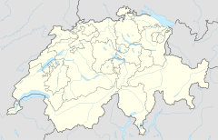
NanoWorld was founded in 2000 with venture capital and strong financial background in Neuchatel, Switzerland, by CEO Manfred Detterbeck, microsystems engineer, master of business and engineering. The company closely collaborates with the IMT (Institute of Microengineering at the EPFL, one of the two Swiss Federal Institutes of Technology), the CSEM (Swiss Center of Electronics and Microtechnology) and the University of Neuchâtel. [1] [2]
In 2002, NanoWorld has acquired the trademark and the technology from Nanosensors (company) considered a "giant" [3] in the AFM probe industry. It is considered one of the top three Swiss nanotechnology companies with a global reputation, inspired by the invention of the atomic force microscope in the IBM research laboratories in Switzerland with a leading market position for AFM probes. [4]
Market research [5] and industry experts [6] confirm that NanoWorld today is the global market leader for AFM probes for scanning probe microscopy (SPM) and atomic force microscopy (AFM). NanoWorld's unique selling proposition is the consistent quality of its AFM probes which is essential for reproducible imaging by atomic force microscope. Its AFM probes cover the full range of atomic force microscopy and Scanning probe microscopy applications. NanoWorld AFM probes are used in research (material science, physics, life science, biology) as well as in industrial applications (semiconductor industry).
Atomic force microscopy (AFM) or scanning force microscopy (SFM) is a very-high-resolution type of scanning probe microscopy (SPM), with demonstrated resolution on the order of fractions of a nanometer, more than 1000 times better than the optical diffraction limit.
Scanning probe microscopy (SPM) is a branch of microscopy that forms images of surfaces using a physical probe that scans the specimen. SPM was founded in 1981, with the invention of the scanning tunneling microscope, an instrument for imaging surfaces at the atomic level. The first successful scanning tunneling microscope experiment was done by Gerd Binnig and Heinrich Rohrer. The key to their success was using a feedback loop to regulate gap distance between the sample and the probe.
Feature-oriented scanning (FOS) is a method of precision measurement of surface topography with a scanning probe microscope in which surface features (objects) are used as reference points for microscope probe attachment. With FOS method, by passing from one surface feature to another located nearby, the relative distance between the features and the feature neighborhood topographies are measured. This approach allows to scan an intended area of a surface by parts and then reconstruct the whole image from the obtained fragments. Beside the mentioned, it is acceptable to use another name for the method – object-oriented scanning (OOS).
Feature-oriented positioning (FOP) is a method of precise movement of the scanning microscope probe across the surface under investigation. With this method, surface features (objects) are used as reference points for microscope probe attachment. Actually, FOP is a simplified variant of the feature-oriented scanning (FOS). With FOP, no topographical image of a surface is acquired. Instead, a probe movement by surface features is only carried out from the start surface point A to the destination point B along some route that goes through intermediate features of the surface. The method may also be referred to by another name—object-oriented positioning (OOP).
Nanometrology is a subfield of metrology, concerned with the science of measurement at the nanoscale level. Nanometrology has a crucial role in order to produce nanomaterials and devices with a high degree of accuracy and reliability in nanomanufacturing.
A recurrence tracking microscope (RTM) is a microscope that is based on the quantum recurrence phenomenon of an atomic wave packet. It is used to investigate the nano-structure on a surface.
Piezoresponse force microscopy (PFM) is a variant of atomic force microscopy (AFM) that allows imaging and manipulation of piezoelectric/ferroelectric materials domains. This is achieved by bringing a sharp conductive probe into contact with a ferroelectric surface and applying an alternating current (AC) bias to the probe tip in order to excite deformation of the sample through the converse piezoelectric effect (CPE). The resulting deflection of the probe cantilever is detected through standard split photodiode detector methods and then demodulated by use of a lock-in amplifier (LiA). In this way topography and ferroelectric domains can be imaged simultaneously with high resolution.
Thermal scanning probe lithography (t-SPL) is a form of scanning probe lithography (SPL) whereby material is structured on the nanoscale using scanning probes, primarily through the application of thermal energy.
Nanosurf AG, headquartered in Liestal, Switzerland, is a developer, manufacturer and supplier of nano-microscopes for industrial and academic research, as well as for educational purposes. Nanosurf's atomic force microscopes (AFM) and scanning tunneling microscopes (STM) are used for metrological surface inspections and for the visualization of structures, and material properties on the nanometer scale.
Photoconductive atomic force microscopy (PC-AFM) is a variant of atomic force microscopy that measures photoconductivity in addition to surface forces.
The technique of vibrational analysis with scanning probe microscopy allows probing vibrational properties of materials at the submicrometer scale, and even of individual molecules. This is accomplished by integrating scanning probe microscopy (SPM) and vibrational spectroscopy. This combination allows for much higher spatial resolution than can be achieved with conventional Raman/FTIR instrumentation. The technique is also nondestructive, requires non-extensive sample preparation, and provides more contrast such as intensity contrast, polarization contrast and wavelength contrast, as well as providing specific chemical information and topography images simultaneously.
Thermochemical nanolithography (TCNL) or thermochemical scanning probe lithography (tc-SPL) is a scanning probe microscopy-based nanolithography technique which triggers thermally activated chemical reactions to change the chemical functionality or the phase of surfaces. Chemical changes can be written very quickly through rapid probe scanning, since no mass is transferred from the tip to the surface, and writing speed is limited only by the heat transfer rate. TCNL was invented in 2007 by a group at the Georgia Institute of Technology. Riedo and collaborators demonstrated that TCNL can produce local chemical changes with feature sizes down to 12 nm at scan speeds up to 1 mm/s.
Nanosensors Inc. is a company that manufactures probes for use in atomic force microscopes (AFM) and scanning probe microscopes (SPM). This private, for profit company was founded November 21, 2018. Nanosensors Inc. is located in Neuchatel, Switzerland.
NanoAndMore is a distributor for AFM cantilevers from NanoWorld, Nanosensors, BudgetSensors, MikroMasch, Opus and nanotools, calibration standards and other products for nanotechnology.
Non-contact atomic force microscopy (nc-AFM), also known as dynamic force microscopy (DFM), is a mode of atomic force microscopy, which itself is a type of scanning probe microscopy. In nc-AFM a sharp probe is moved close to the surface under study, the probe is then raster scanned across the surface, the image is then constructed from the force interactions during the scan. The probe is connected to a resonator, usually a silicon cantilever or a quartz crystal resonator. During measurements the sensor is driven so that it oscillates. The force interactions are measured either by measuring the change in amplitude of the oscillation at a constant frequency just off resonance or by measuring the change in resonant frequency directly using a feedback circuit to always drive the sensor on resonance.
Franz Josef Gießibl is a German physicist and university professor at the University of Regensburg.
AFM-IR or infrared nanospectroscopy is one of a family of techniques that are derived from a combination of two parent instrumental techniques. AFM-IR combines the chemical analysis power of infrared spectroscopy and the high-spatial resolution of scanning probe microscopy (SPM). The term was first used to denote a method that combined a tuneable free electron laser with an atomic force microscope equipped with a sharp probe that measured the local absorption of infrared light by a sample with nanoscale spatial resolution.
A probe tip is an instrument used in scanning probe microscopes (SPMs) to scan the surface of a sample and make nano-scale images of surfaces and structures. The probe tip is mounted on the end of a cantilever and can be as sharp as a single atom. In microscopy, probe tip geometry and the composition of both the tip and the surface being probed directly affect resolution and imaging quality. Tip size and shape are extremely important in monitoring and detecting interactions between surfaces. SPMs can precisely measure electrostatic forces, magnetic forces, chemical bonding, Van der Waals forces, and capillary forces. SPMs can also reveal the morphology and topography of a surface.
Multi-tip scanning tunneling microscopy extends scanning tunneling microscopy (STM) from imaging to dedicated electrical measurements at the nanoscale like a ″multimeter at the nanoscale″. In materials science, nanoscience, and nanotechnology, it is desirable to measure electrical properties at a particular position of the sample. For this purpose, multi-tip STMs in which several tips are operated independently have been developed. Apart from imaging the sample, the tips of a multi-tip STM are used to form contacts to the sample at desired locations and to perform local electrical measurements.
Bimodal Atomic Force Microscopy is an advanced atomic force microscopy technique characterized by generating high-spatial resolution maps of material properties. Topography, deformation, elastic modulus, viscosity coefficient or magnetic field maps might be generated. Bimodal AFM is based on the simultaneous excitation and detection of two eigenmodes (resonances) of a force microscope microcantilever.