Perspective view of nanomesh, whose structure ends at the back of the figure. The distance between two pore centers is 3.2nm, and the pores are 0.05nm deep.
The nanomesh is an inorganic nanostructured two-dimensional material, similar to graphene. It was discovered in 2003 at the University of Zurich, Switzerland.[1]
The nanomesh looks like an assembly of hexagonal pores[3] (see right image) at the nanometer (nm) scale. The distance between two pore centers is only 3.2nm, whereas each pore has a diameter of about 2nm and is 0.05nm deep. The lowest regions bind strongly to the underlying metal, while the wires[3] (highest regions) are only bound to the surface through strong cohesive forces within the layer itself.
The boron nitride nanomesh is not only stable under vacuum,[1] air[4] and some liquids,[5][6] but also up to temperatures of 796°C (1070 K).[1] In addition it shows the extraordinary ability to trap molecules[5] and metallic clusters,[2] which have similar sizes to the nanomesh pores, forming a well-ordered array. These characteristics may provide applications of the material in areas like, surface functionalisation, spintronics, quantum computing and data storage media like hard drives.
Structure
Cross-section of nanomesh on rhodium showing pore and wire regions
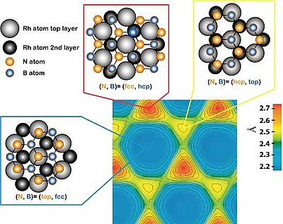
The unit cell of the h-BN nanomesh consists of 13x13 BN or 12x12 Rh atoms with a lattice constant of 3.2nm. In a cross-section it means that 13 boron or nitrogen atoms are sitting on 12 rhodium atoms. This implies a modification of the relative positions of each BN towards the substrate atoms within a unit cell, where some bonds are more attractive or repulsive than other (site selective bonding), what induces the corrugation of the nanomesh (see right image with pores and wires).
The nanomesh corrugation amplitude of 0.05nm causes a strong effect on the electronic structure, where two distinct BN regions are observed. They are easily recognized in the lower right image, which is a scanning tunneling microscopy (STM) measurement, as well as in the lower left image representing a theoretical calculation of the same area. A strongly bounded region assigned to the pores is visible in blue in the left image below (center of bright rings in the right image) and a weakly bound region assigned to the wires appears yellow-red in the left image below (area in-between rings in the right image).
The right image shows the boron nitride nanomesh measured by STM at 77K, where each "ball" represents one N atom. The center of each ring corresponds to the center of the pores.
The left image is the theoretical calculation of the same area, where the N height relative to the underlying substrate is given. The exact arrangement of Rh, N and B atoms is given for three different areas (blue: pores, yellow-red: wires).
Naphthalocyanine molecules evaporated onto the nanomesh. They only adsorb in pores, forming a well-defined pattern.
The nanomesh is stable under a wide range of environments like air, water and electrolytes among others. It is also temperature resistant since it does not decompose in temperatures up to 1275K under a vacuum. In addition to these exceptional stabilities, the nanomesh shows the extraordinary ability to act as a scaffold for metallic nanoclusters and to trap molecules forming a well-ordered array.
In the case of gold (Au), its evaporation on the nanomesh leads to formation of well-defined round Au nanoparticles, which are centered at the nanomesh pores.
The STM figure on the right shows Naphthalocyanine (Nc) molecules, which were vapor-deposited onto the nanomesh. These planar molecules have a diameter of about 2nm, whose size is comparable to that of the nanomesh pores (see upper inset). It is spectacularly visible how the molecules form a well-ordered array with the periodicity of the nanomesh (3.22nm). The lower inset shows a region of this substrate with higher resolution, where individual molecules are trapped inside the pores. In addition, the molecules seem to keep their native conformation, what means that their functionality is kept, which is nowadays a challenge in nanoscience.
The substrate is kept at a temperature of 796°C (1070 K) when borazine is introduced in the vacuum chamber at a dose of about 40 L (1 Langmuir = 10−6torr sec). A typical borazine vapor pressure inside the ultrahigh vacuum chamber during the exposure is 3x10⁻⁷mbar.
After cooling down to room temperature, the regular mesh structure is observed using different experimental techniques. Scanning tunneling microscopy (STM) gives a direct look on the local real space structure of the nanomesh, while low energy electron diffraction (LEED) gives information about the surface structures ordered over the whole sample. Ultraviolet photoelectron spectroscopy (UPS) gives information about the electronic states in the outermost atomic layers of a sample, i.e. electronic information of the top substrate layers and the nanomesh.
CVD of borazine on other substrates has not led so far to the formation of a corrugated nanomesh. A flat BN layer is observed on nickel[8] and palladium,[9][10] whereas stripped structures appear on molybdenum[11] instead.
1 2 3 4 A. Goriachko; He, Y; Knapp, M; Over, H; etal. (2007). "Self-assembly of a hexagonal boron nitride nanomesh on Ru(0001)". Langmuir. 23 (6): 2928–2931. doi:10.1021/la062990t. PMID17286422.
1 2 In the literature different words referring to similar concepts can be found. Below is a summary of them:
Pores, apertures, holes: areas of the nanomesh laying the closest to the underlying substrate due to a strong attraction. They form depressions, which are 0.05 nm deep and have a hexagonal shape.
Wires: areas of the nanomesh referring to the border of the pores, which lay the farer away to the underlying substrate and therefore represent the upper part of the nanomesh.
Boron nitride is a thermally and chemically resistant refractory compound of boron and nitrogen with the chemical formula BN. It exists in various crystalline forms that are isoelectronic to a similarly structured carbon lattice. The hexagonal form corresponding to graphite is the most stable and soft among BN polymorphs, and is therefore used as a lubricant and an additive to cosmetic products. The cubic variety analogous to diamond is called c-BN; it is softer than diamond, but its thermal and chemical stability is superior. The rare wurtzite BN modification is similar to lonsdaleite but slightly softer than the cubic form.
Boron is a chemical element with the symbol B and atomic number 5. In its crystalline form it is a brittle, dark, lustrous metalloid; in its amorphous form it is a brown powder. As the lightest element of the boron group it has three valence electrons for forming covalent bonds, resulting in many compounds such as boric acid, the mineral sodium borate, and the ultra-hard crystals of boron carbide and boron nitride.
Epitaxy refers to a type of crystal growth or material deposition in which new crystalline layers are formed with one or more well-defined orientations with respect to the crystalline seed layer. The deposited crystalline film is called an epitaxial film or epitaxial layer. The relative orientation(s) of the epitaxial layer to the seed layer is defined in terms of the orientation of the crystal lattice of each material. For most epitaxial growths, the new layer is usually crystalline and each crystallographic domain of the overlayer must have a well-defined orientation relative to the substrate crystal structure. Epitaxy can involve single-crystal structures, although grain-to-grain epitaxy has been observed in granular films. For most technological applications, single domain epitaxy, which is the growth of an overlayer crystal with one well-defined orientation with respect to the substrate crystal, is preferred. Epitaxy can also play an important role while growing superlattice structures.
Nanomaterials describe, in principle, materials of which a single unit is sized between 1 and 100 nm.
Aluminium nitride (AlN) is a solid nitride of aluminium. It has a high thermal conductivity of up to 321 W/(m·K) and is an electrical insulator. Its wurtzite phase (w-AlN) has a band gap of ~6 eV at room temperature and has a potential application in optoelectronics operating at deep ultraviolet frequencies.
A superhard material is a material with a hardness value exceeding 40 gigapascals (GPa) when measured by the Vickers hardness test. They are virtually incompressible solids with high electron density and high bond covalency. As a result of their unique properties, these materials are of great interest in many industrial areas including, but not limited to, abrasives, polishing and cutting tools, disc brakes, and wear-resistant and protective coatings.
Borazine, also known as borazole, is a polar inorganic compound with the chemical formula B3H6N3. In this cyclic compound, the three BH units and three NH units alternate. The compound is isoelectronic and isostructural with benzene. For this reason borazine is sometimes referred to as “inorganic benzene”. Like benzene, borazine is a colourless liquid with an aromatic smell.
Atomic layer deposition (ALD) is a thin-film deposition technique based on the sequential use of a gas-phase chemical process; it is a subclass of chemical vapour deposition. The majority of ALD reactions use two chemicals called precursors. These precursors react with the surface of a material one at a time in a sequential, self-limiting, manner. A thin film is slowly deposited through repeated exposure to separate precursors. ALD is a key process in fabricating semiconductor devices, and part of the set of tools for synthesising nanomaterials.
Boron arsenide is a chemical compound involving boron and arsenic, usually with a chemical formula BAs. Other boron arsenide compounds are known, such as the subarsenide B12As2. Chemical synthesis of cubic BAs is very challenging and its single crystal forms usually have defects.
Rhenium diboride (ReB2) is a synthetic superhard material. It was first synthesized in 1962 and re-emerged recently due to hopes of achieving high hardness comparable to that of diamond. The reported ultrahigh hardness has been questioned, although this is a matter of definition as in the initial test rhenium diboride was able to scratch diamond.
Dry lubricants or solid lubricants are materials that, despite being in the solid phase, are able to reduce friction between two surfaces sliding against each other without the need for a liquid oil medium.
A nanosheet is a two-dimensional nanostructure with thickness in a scale ranging from 1 to 100 nm.
Potential graphene applications include lightweight, thin, and flexible electric/photonics circuits, solar cells, and various medical, chemical and industrial processes enhanced or enabled by the use of new graphene materials.
In materials science, the term single-layer materials or 2D materials refers to crystalline solids consisting of a single layer of atoms. These materials are promising for some applications but remain the focus of research. Single-layer materials derived from single elements generally carry the -ene suffix in their names, e.g. graphene. Single-layer materials that are compounds of two or more elements have -ane or -ide suffixes. 2D materials can generally be categorized as either 2D allotropes of various elements or as compounds.
Molybdenum(IV) telluride, molybdenum ditelluride or just molybdenum telluride is a compound of molybdenum and tellurium with formula MoTe2, corresponding to a mass percentage of 27.32% molybdenum and 72.68% tellurium. It can crystallise in two dimensional sheets which can be thinned down to monolayers that are flexible and almost transparent. It is a semiconductor, and can fluoresce. It is part of a class of materials called transition metal dichalcogenides. As a semiconductor the band gap lies in the infrared region. This raises the potential use as a semiconductor in electronics or an infrared detector.
Boron nitride aerogel is an aerogel made of highly porous boron nitride (BN). It typically consists of a mixture of deformed boron nitride nanotubes and nanosheets. It can have a density as low as 0.6 mg/cm3 and a specific surface area as high as 1050 m2/g, and therefore has potential applications as an absorbent, catalyst support and gas storage medium. BN aerogels are highly hydrophobic and can absorb up to 160 times their mass in oil. They are resistant to oxidation in air at temperatures up to 1200 °C, and hence can be reused after the absorbed oil is burned out by flame. BN aerogels can be prepared by template-assisted chemical vapor deposition at a temperature ~900 °C using borazine as the feed gas. Alternatively it can be produced by ball milling h-BN powder, ultrasonically dispersing it in water, and freeze-drying the dispersion.
Boron nitride nanosheet is a two-dimensional crystalline form of the hexagonal boron nitride (h-BN), which has a thickness of one to few atomic layers. It is similar in geometry to its all-carbon analog graphene, but has very different chemical and electronic properties – contrary to the black and highly conducting graphene, BN nanosheets are electrical insulators with a band gap of ~5.9 eV, and therefore appear white in color.
A graphene morphology is any of the structures related to, and formed from, single sheets of graphene. 'Graphene' is typically used to refer to the crystalline monolayer of the naturally occurring material graphite. Due to quantum confinement of electrons within the material at these low dimensions, small differences in graphene morphology can greatly impact the physical and chemical properties of these materials. Commonly studied graphene morphologies include the monolayer sheets, bilayer sheets, graphene nanoribbons and other 3D structures formed from stacking of the monolayer sheets.
Two dimensional hexagonal boron nitride is a material of comparable structure to graphene with potential applications in e.g. photonics., fuel cells and as a substrate for two-dimensional heterostructures. 2D h-BN is isostructural to graphene, but where graphene is conductive, 2D h-BN is a wide-gap insulator.
Low-energy plasma-enhanced chemical vapor deposition (LEPECVD) is a plasma-enhanced chemical vapor deposition technique used for the epitaxial deposition of thin semiconductor films. A remote low energy, high density DC argon plasma is employed to efficiently decompose the gas phase precursors while leaving the epitaxial layer undamaged, resulting in high quality epilayers and high deposition rates.
This page is based on this Wikipedia article Text is available under the CC BY-SA 4.0 license; additional terms may apply. Images, videos and audio are available under their respective licenses.