
Microelectromechanical systems (MEMS), also written as micro-electro-mechanical systems and the related micromechatronics and microsystems constitute the technology of microscopic devices, particularly those with moving parts. They merge at the nanoscale into nanoelectromechanical systems (NEMS) and nanotechnology. MEMS are also referred to as micromachines in Japan and microsystem technology (MST) in Europe.
In integrated circuit manufacturing, photolithography or optical lithography is a general term used for techniques that use light to produce minutely patterned thin films of suitable materials over a substrate, such as a silicon wafer, to protect selected areas of it during subsequent etching, deposition, or implantation operations. Typically, ultraviolet light is used to transfer a geometric design from an optical mask to a light-sensitive chemical (photoresist) coated on the substrate. The photoresist either breaks down or hardens where it is exposed to light. The patterned film is then created by removing the softer parts of the coating with appropriate solvents.
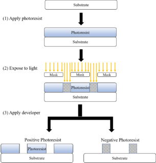
A photoresist is a light-sensitive material used in several processes, such as photolithography and photoengraving, to form a patterned coating on a surface. This process is crucial in the electronic industry.

Polydimethylsiloxane (PDMS), also known as dimethylpolysiloxane or dimethicone, belongs to a group of polymeric organosilicon compounds that are commonly referred to as silicones. PDMS is the most widely used silicon-based organic polymer, as its versatility and properties lead to many applications.
In chemistry, an interhalogen compound is a molecule which contains two or more different halogen atoms and no atoms of elements from any other group.
Bulk micromachining is a process used to produce micromachinery or microelectromechanical systems (MEMS).

An ion beam is a type of charged particle beam consisting of ions. Ion beams have many uses in electronics manufacturing and other industries. A variety of ion beam sources exists, some derived from the mercury vapor thrusters developed by NASA in the 1960s. The most common ion beams are of singly-charged ions.

A stepper is a device used in the manufacture of integrated circuits (ICs) that is similar in operation to a slide projector or a photographic enlarger. The term "stepper" is short for step-and-repeat camera. Steppers are an essential part of the complex process, called photolithography, that creates millions of microscopic circuit elements on the surface of chips of silicon. These chips form the heart of ICs such as computer processors, memory chips, and many other devices.
Nanoimprint lithography (NIL) is a method of fabricating nanometer scale patterns. It is a simple nanolithography process with low cost, high throughput and high resolution. It creates patterns by mechanical deformation of imprint resist and subsequent processes. The imprint resist is typically a monomer or polymer formulation that is cured by heat or UV light during the imprinting. Adhesion between the resist and the template is controlled to allow proper release.
Porous silicon is a form of the chemical element silicon that has introduced nanopores in its microstructure, rendering a large surface to volume ratio in the order of 500 m2/cm3.

Microfabrication is the process of fabricating miniature structures of micrometre scales and smaller. Historically, the earliest microfabrication processes were used for integrated circuit fabrication, also known as "semiconductor manufacturing" or "semiconductor device fabrication". In the last two decades microelectromechanical systems (MEMS), microsystems, micromachines and their subfields, microfluidics/lab-on-a-chip, optical MEMS, RF MEMS, PowerMEMS, BioMEMS and their extension into nanoscale have re-used, adapted or extended microfabrication methods. Flat-panel displays and solar cells are also using similar techniques.
Nanochemistry is the combination of chemistry and nano science. Nanochemistry is associated with synthesis of building blocks which are dependent on size, surface, shape and defect properties. Nanochemistry is being used in chemical, materials and physical, science as well as engineering, biological and medical applications. Nanochemistry and other nanoscience fields have the same core concepts but the usages of those concepts are different.

Microcontact printing is a form of soft lithography that uses the relief patterns on a master polydimethylsiloxane (PDMS) stamp or Urethane rubber micro stamp to form patterns of self-assembled monolayers (SAMs) of ink on the surface of a substrate through conformal contact as in the case of nanotransfer printing (nTP). Its applications are wide-ranging including microelectronics, surface chemistry and cell biology.

Etching is used in microfabrication to chemically remove layers from the surface of a wafer during manufacturing. Etching is a critically important process module, and every wafer undergoes many etching steps before it is complete.

Glass etching, or "French embossing", is a popular technique developed during the mid-1800s that is still widely used in both residential and commercial spaces today. Glass etching comprises the techniques of creating art on the surface of glass by applying acidic, caustic, or abrasive substances. Traditionally this is done after the glass is blown or cast, although mold-etching has replaced some forms of surface etching. The removal of minute amounts of glass causes the characteristic rough surface and translucent quality of frosted glass.
Microlithography is a general name for any manufacturing process that can create a minutely patterned thin film of protective materials over a substrate, such as a silicon wafer, in order to protect selected areas of it during subsequent etching, deposition, or implantation operations. The term is normally used for processes that can reliably produce features of microscopic size, such as 10 micrometres or less. The term nanolithography may be used to designate processes that can produce nanoscale features, such as less than 100 nanometres.
![PDMS stamp Patterned silicone piece]](https://upload.wikimedia.org/wikipedia/commons/thumb/d/db/Sarfus.SoftLitho.Streptavidin.jpg/320px-Sarfus.SoftLitho.Streptavidin.jpg)
PDMS stamps are pieces of polydimethylsiloxane (PDMS), a silicone, that have been patterned usually against a master mask to form a relief pattern used in soft lithography. This PDMS stamp can be used in either its current form as a relief surface for techniques such as microcontact printing or can also be attached to an external source by tubing so that liquid may be passed through channels on its surface. In this second case it will often be laminated to a surface so that chemistry can be performed on that surface producing a pattern of the PDMS stamp on to the surface. Alternatively a PDMS stamp can be laminated to a second piece of PDMS to form a contained device. It is possible to pattern PDMS with nanometre resolution. PDMS stamps can be procured from some commercial sources such as Research Micro Stamps. Many techniques have been developed to modify the basic setups to perform a range of tasks such as assays on small volumes. These kinds of devices are often referred to as microfluidic devices. Because of the small dimensions of these devices flow is laminar not turbulent which can lead to many useful properties; however, this reduces the ability of fluid streams to mix.
Bio-MEMS is an abbreviation for biomedical microelectromechanical systems. Bio-MEMS have considerable overlap, and is sometimes considered synonymous, with lab-on-a-chip (LOC) and micro total analysis systems (μTAS). Bio-MEMS is typically more focused on mechanical parts and microfabrication technologies made suitable for biological applications. On the other hand, lab-on-a-chip is concerned with miniaturization and integration of laboratory processes and experiments into single chips. In this definition, lab-on-a-chip devices do not strictly have biological applications, although most do or are amenable to be adapted for biological purposes. Similarly, micro total analysis systems may not have biological applications in mind, and are usually dedicated to chemical analysis. A broad definition for bio-MEMS can be used to refer to the science and technology of operating at the microscale for biological and biomedical applications, which may or may not include any electronic or mechanical functions. The interdisciplinary nature of bio-MEMS combines material sciences, clinical sciences, medicine, surgery, electrical engineering, mechanical engineering, optical engineering, chemical engineering, and biomedical engineering. Some of its major applications include genomics, proteomics, molecular diagnostics, point-of-care diagnostics, tissue engineering, single cell analysis and implantable microdevices.
Direct bonding, or fusion bonding, describes a wafer bonding process without any additional intermediate layers. The bonding process is based on chemical bonds between two surfaces of any material possible meeting numerous requirements. These requirements are specified for the wafer surface as sufficiently clean, flat and smooth. Otherwise unbonded areas so called voids, i.e. interface bubbles, can occur.
Vapor etching refers to a process used in the fabrication of Microelectromechanical systems (MEMS) and Nanoelectromechanical systems (NEMS). Sacrificial layers are isotropically etched using gaseous acids such as Hydrogen fluoride and Xenon difluoride to release the free standing components of the device.
Perring M., Mitchell, M., Kenis P. J. A., Bowden N. B., Chem. Mat200719(11), 2903
