In integrated circuit manufacturing, photolithography or optical lithography is a general term used for techniques that use light to produce minutely patterned thin films of suitable materials over a substrate, such as a silicon wafer, to protect selected areas of it during subsequent etching, deposition, or implantation operations. Typically, ultraviolet light is used to transfer a geometric design from an optical mask to a light-sensitive chemical (photoresist) coated on the substrate. The photoresist either breaks down or hardens where it is exposed to light. The patterned film is then created by removing the softer parts of the coating with appropriate solvents, also known in this case as developers.

An optical coating is one or more thin layers of material deposited on an optical component such as a lens, prism or mirror, which alters the way in which the optic reflects and transmits light. These coatings have become a key technology in the field of optics. One type of optical coating is an anti-reflective coating, which reduces unwanted reflections from surfaces, and is commonly used on spectacle and camera lenses. Another type is the high-reflector coating, which can be used to produce mirrors that reflect greater than 99.99% of the light that falls on them. More complex optical coatings exhibit high reflection over some range of wavelengths, and anti-reflection over another range, allowing the production of dichroic thin-film filters.

A photomask is an opaque plate with transparent areas that allow light to shine through in a defined pattern. Photomasks are commonly used in photolithography for the production of integrated circuits to produce a pattern on a thin wafer of material. Several masks are used in turn, each one reproducing a layer of the completed design, and together known as a mask set.

Immersion lithography is a photolithography resolution enhancement technique for manufacturing integrated circuits (ICs) that replaces the usual air gap between the final lens and the wafer surface with a liquid medium that has a refractive index greater than one. The resolution is increased by a factor equal to the refractive index of the liquid. Current immersion lithography tools use highly purified water for this liquid, achieving feature sizes below 45 nanometers.
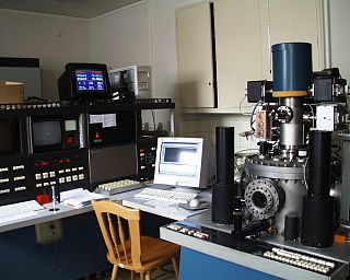
Electron-beam lithography is the practice of scanning a focused beam of electrons to draw custom shapes on a surface covered with an electron-sensitive film called a resist (exposing). The electron beam changes the solubility of the resist, enabling selective removal of either the exposed or non-exposed regions of the resist by immersing it in a solvent (developing). The purpose, as with photolithography, is to create very small structures in the resist that can subsequently be transferred to the substrate material, often by etching.
Masklesslithography (MPL) is a photomask-less photolithography-like technology used to project or focal-spot write the image pattern onto a chemical resist-coated substrate by means of UV radiation or electron beam.
Nanolithography (NL) is a growing field of techniques within nanotechnology dealing with the engineering of nanometer-scale structures on various materials.

Extreme ultraviolet lithography is an optical lithography technology used in semiconductor device fabrication to make integrated circuits (ICs). It uses extreme ultraviolet (EUV) wavelengths near 13.5 nm, using a laser-pulsed tin (Sn) droplet plasma, to produce a pattern by using a reflective photomask to expose a substrate covered by photoresist. It is currently applied only in the most advanced semiconductor device fabrication.
Next-generation lithography or NGL is a term used in integrated circuit manufacturing to describe the lithography technologies in development which are intended to replace current techniques. The term applies to any lithography method which uses a shorter-wavelength light or beam type than the current state of the art, such as X-ray lithography, electron beam lithography, focused ion beam lithography, and nanoimprint lithography. The term may also be used to describe techniques which achieve finer resolution features from an existing light wavelength.

A stepper is a device used in the manufacture of integrated circuits (ICs) that is similar in operation to a slide projector or a photographic enlarger. Stepper is short for step-and-repeat camera. Steppers are an essential part of the complex process, called photolithography, which creates millions of microscopic circuit elements on the surface of silicon wafers out of which chips are made. These chips form the heart of ICs such as computer processors, memory chips, and many other devices.
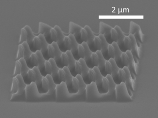
Nanoimprint lithography (NIL) is a method of fabricating nanometer scale patterns. It is a simple nanolithography process with low cost, high throughput and high resolution. It creates patterns by mechanical deformation of imprint resist and subsequent processes. The imprint resist is typically a monomer or polymer formulation that is cured by heat or UV light during the imprinting. Adhesion between the resist and the template is controlled to allow proper release.

Optical proximity correction (OPC) is a photolithography enhancement technique commonly used to compensate for image errors due to diffraction or process effects. The need for OPC is seen mainly in the making of semiconductor devices and is due to the limitations of light to maintain the edge placement integrity of the original design, after processing, into the etched image on the silicon wafer. These projected images appear with irregularities such as line widths that are narrower or wider than designed, these are amenable to compensation by changing the pattern on the photomask used for imaging. Other distortions such as rounded corners are driven by the resolution of the optical imaging tool and are harder to compensate for. Such distortions, if not corrected for, may significantly alter the electrical properties of what was being fabricated. Optical proximity correction corrects these errors by moving edges or adding extra polygons to the pattern written on the photomask. This may be driven by pre-computed look-up tables based on width and spacing between features or by using compact models to dynamically simulate the final pattern and thereby drive the movement of edges, typically broken into sections, to find the best solution,. The objective is to reproduce the original layout drawn by the designer on the semiconductor wafer as well as possible.
Resolution enhancement technologies are methods used to modify the photomasks in the lithographic processes used to make integrated circuits to compensate for limitations in the optical resolution of the projection systems. These processes allow the creation of features well beyond the limit that would normally apply due to the Rayleigh criterion. Modern technologies allow the creation of features on the order of 5 nanometers (nm), far below the normal resolution possible using deep ultraviolet (DUV) light.

Optical tomography is a form of computed tomography that creates a digital volumetric model of an object by reconstructing images made from light transmitted and scattered through an object. Optical tomography is used mostly in medical imaging research. Optical tomography in industry is used as a sensor of thickness and internal structure of semiconductors.
Contact lithography, also known as contact printing, is a form of photolithography whereby the image to be printed is obtained by illumination of a photomask in direct contact with a substrate coated with an imaging photoresist layer.
A mask shop is a factory which manufactures photomasks for use in the semiconductor industry. There are two distinct types found in the trade. Captive mask shops are in-house operations owned by the biggest semiconductor corporations, while merchant mask shops make masks for most of the industry.

Multiple patterning is a class of technologies for manufacturing integrated circuits (ICs), developed for photolithography to enhance the feature density. It is expected to be necessary for the 10 nm and 7 nm node semiconductor processes and beyond. The premise is that a single lithographic exposure may not be enough to provide sufficient resolution. Hence additional exposures would be needed, or else positioning patterns using etched feature sidewalls would be necessary.
Computational lithography is the set of mathematical and algorithmic approaches designed to improve the resolution attainable through photolithography. Computational lithography came to the forefront of photolithography technologies in 2008 when the semiconductor industry faced challenges associated with the transition to a 22 nanometer CMOS microfabrication process and has become instrumental in further shrinking the design nodes and topology of semiconductor transistor manufacturing.
In semiconductor manufacturing, the International Technology Roadmap for Semiconductors defines the 7 nm process as the MOSFET technology node following the 10 nm node. It is based on FinFET technology, a type of multi-gate MOSFET technology.

Carl Zeiss SMT GmbH comprises the Semiconductor Manufacturing Technology business group of ZEISS and develops and produces equipment for the manufacture of microchips. The company is majority owned by Carl Zeiss AG, with a 24.9% minority stake by ASML Holding.


