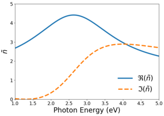
A. R. Forouhi and I. Bloomer deduced dispersion equations for the refractive index, n, and extinction coefficient, k, which were published in 1986[1] and 1988.[2] The 1986 publication relates to amorphous materials, while the 1988 publication relates to crystalline. Subsequently, in 1991, their work was included as a chapter in The Handbook of Optical Constants.[3] The Forouhi–Bloomer dispersion equations describe how photons of varying energies interact with thin films. When used with a spectroscopic reflectometry tool, the Forouhi–Bloomer dispersion equations specify n and k for amorphous and crystalline materials as a function of photon energy E. Values of n and k as a function of photon energy, E, are referred to as the spectra of n and k, which can also be expressed as functions of the wavelength of light, λ, since E = hc/λ. The symbol h is the Planck constant and c, the speed of light in vacuum. Together, n and k are often referred to as the "optical constants" of a material (though they are not constants since their values depend on photon energy).
The derivation of the Forouhi–Bloomer dispersion equations is based on obtaining an expression for k as a function of photon energy, symbolically written as k(E), starting from first principles quantum mechanics and solid state physics. An expression for n as a function of photon energy, symbolically written as n(E), is then determined from the expression for k(E) in accordance to the Kramers–Kronig relations[4] which states that n(E) is the Hilbert transform of k(E).
The Forouhi–Bloomer dispersion equations for n(E) and k(E) of amorphous materials are given as:
The five parameters A, B, C, Eg, and n(∞) each have physical significance.[1][3]Eg is the optical energy band gap of the material. A, B, and C depend on the band structure of the material. They are positive constants such that 4C − B2 > 0. Finally, n(∞), a constant greater than unity, represents the value of n at E = ∞. The parameters B0 and C0 in the equation for n(E) are not independent parameters, but depend on A, B, C, and Eg. They are given by:
where
Thus, for amorphous materials, a total of five parameters are sufficient to fully describe the dependence of both n and k on photon energy, E.
For crystalline materials which have multiple peaks in their n and k spectra, the Forouhi–Bloomer dispersion equations can be extended as follows:
The number of terms in each sum, q, is equal to the number of peaks in the n and k spectra of the material. Every term in the sum has its own values of the parameters A, B, C, Eg, as well as its own values of B0 and C0. Analogous to the amorphous case, the terms all have physical significance.[2][3]
Characterizing thin films
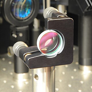
The refractive index (n) and extinction coefficient (k) are related to the interaction between a material and incident light, and are associated with refraction and absorption (respectively). They can be considered as the "fingerprint of the material". Thin film material coatings on various substrates provide important functionalities for the microfabrication industry, and the n, k, as well as the thickness, t, of these thin film constituents must be measured and controlled to allow for repeatable manufacturing.
The Forouhi–Bloomer dispersion equations for n and k were originally expected to apply to semiconductors and dielectrics, whether in amorphous, polycrystalline, or crystalline states. However, they have been shown to describe the n and k spectra of transparent conductors,[5] as well as metallic compounds.[6][7][8][9][10][11][12][13][14][15] The formalism for crystalline materials was found to also apply to polymers,[16][17][18] which consist of long chains of molecules that do not form a crystallographic structure in the classical sense.
Other dispersion models that can be used to derive n and k, such as the Tauc–Lorentz model, can be found in the literature.[19][20] Two well-known models—Cauchy and Sellmeier—provide empirical expressions for n valid over a limited measurement range, and are only useful for non-absorbing films where k=0. Consequently, the Forouhi–Bloomer formulation has been used for measuring thin films in various applications.[5][6][7][8][9][10][11][12][13][14][15][16][17][18][19][20]
In the following discussions, all variables of photon energy, E, will be described in terms of wavelength of light, λ, since experimentally variables involving thin films are typically measured over a spectrum of wavelengths. The n and k spectra of a thin film cannot be measured directly, but must be determined indirectly from measurable quantities that depend on them. Spectroscopic reflectance, R(λ), is one such measurable quantity. Another, is spectroscopic transmittance, T(λ), applicable when the substrate is transparent. Spectroscopic reflectance of a thin film on a substrate represents the ratio of the intensity of light reflected from the sample to the intensity of incident light, measured over a range of wavelengths, whereas spectroscopic transmittance, T(λ), represents the ratio of the intensity of light transmitted through the sample to the intensity of incident light, measured over a range of wavelengths; typically, there will also be a reflected signal, R(λ), accompanying T(λ).
The measurable quantities, R(λ) and T(λ) depend not only on n(λ) and k(λ) of the film, but also on film thickness, t, and n(λ) and k(λ) of the substrate. For a silicon substrate, the n(λ) and k(λ) values are known and are taken as a given input. The challenge of characterizing thin films involves extracting t, n(λ) and k(λ) of the film from the measurement of R(λ) and/or T(λ). This can be achieved by combining the Forouhi–Bloomer dispersion equations for n(λ) and k(λ) with the Fresnel equations for the reflection and transmission of light at an interface[21] to obtain theoretical, physically valid, expressions for reflectance and transmittance. In so doing, the challenge is reduced to extracting the five parameters A, B, C, Eg, and n(∞) that constitute n(λ) and k(λ), along with film thickness, t, by using a nonlinear least squares regression analysis[22][23] fitting procedure. The fitting procedure entails an iterative improvement of the values of A, B, C, Eg, n(∞), t, in order to reduce the sum of the squares of the errors between the theoretical R(λ) or theoretical T(λ) and the measured spectrum of R(λ) or T(λ).
Besides spectroscopic reflectance and transmittance, spectroscopic ellipsometry can also be used in an analogous way to characterize thin films and determine t, n(λ) and k(λ).
Measurement examples
The following examples show the versatility of using the Forouhi–Bloomer dispersion equations to characterize thin films using a tool based on near-normal incident spectroscopic reflectance. Near-normal spectroscopic transmittance is also used when the substrate is transparent. The n(λ) and k(λ) spectra of each film are obtained along with film thickness, over a wide range of wavelengths from deep ultraviolet to near infrared wavelengths (190–1000nm).
In the following examples, the notation for theoretical and measured reflectance in the spectral plots is expressed as "R-theor" and "R-meas", respectively.
Below are schematics depicting the thin film measurement process:
Thin film characterization involves determining the film's thickness (t) plus its refractive index (n) and extinction coefficient (k) over as wide a wavelength range as possible, preferably covering ultra-violet through near infra-red wavelengths (190–1000nm). By measuring near-normal incident reflectance (R) of the film (from 190 to 1000nm), and analyzing R using the Forouhi–Bloomer dispersion equations, the film can be completely characterized.
The Forouhi–Bloomer dispersion equations in combination with Rigorous Coupled-Wave Analysis (RCWA) have also been used to obtain detailed profile information (depth, CD, sidewall angle) of trench structures. In order to extract structure information, polarized broadband reflectance data, Rs and Rp, must be collected over a large wavelength range from a periodic structure (grating), and then analyzed with a model that incorporates Forouhi–Bloomer dispersion equations and RCWA. Inputs into the model include grating pitch and n and k spectra of all materials within the structure, while outputs can include Depth, CDs at multiple locations, and even sidewall angle. The n and k spectra of such materials can be obtained in accordance with the methodology described in this section for thin film measurements.
Below are schematics depicting the measurement process for trench structures. Examples of trench measurements then follow.
The key properties of trench structures are trench depth, critical dimensions, plus profile (or sidewall angle). The term "critical dimension" is usually abbreviated as "CD". CDs signify widths of the trench at various levels inside the trench – top, middle, and bottom of trench. These key properties can be determined by measuring polarized reflectance Rs and Rp over as wide a wavelength range as possible, preferably covering ultra-violet through near infra-red wavelengths (190–1000nm). Analysis of the measured Rs and Rp, based on the Forouhi–Bloomer dispersion equations (to characterize any films within the trench structure), combined with Rigorous Coupled Wave Analysis (RCWA) (to determine the geometry), will provide trench depth, CDs and profiles.
Example 1: Amorphous silicon on oxidized silicon substrate (a-Si/SiO2/Si-Sub)
Ex. 1: Reflectance spectra collected over 190–1000nm wavelength range for an amorphous silicon film (a-Si) on an oxidized silicon substrate (SiO2/Si-Sub) plus the n(λ) and k(λ) spectra of the a-Si film. The film thickness was found to be 1147nm. The thicknesses of a-Si and SiO2 films, plus the n(λ) and k(λ) spectra of the a-Si were all simultaneously determined. The n(λ) and k(λ) spectra of the SiO2 film was held fixed.
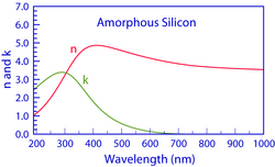
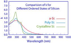
Ex. 1: Amorphous materials typically exhibit one broad maximum in their n(λ) and k(λ) spectra. As a material transitions from the amorphous state to the fully crystalline state, the broad maximum sharpens up and other sharp peaks start to appear in the n(λ) and k(λ) spectra. This is demonstrated for the case of amorphous silicon progressing to poly-silicon and further progressing to crystalline silicon.
Example 1 shows one broad maximum in the n(λ) and k(λ) spectra of the a-Si film, as is expected for amorphous materials. As a material transitions toward crystallinity, the broad maximum gives way to several sharper peaks in its n(λ) and k(λ) spectra, as demonstrated in the graphics.
When the measurement involves two or more films in a stack of films, the theoretical expression for reflectance must be expanded to include the n(λ) and k(λ) spectra, plus thickness, t, of each film. However, the regression may not converge to unique values of the parameters, due to the non-linear nature of the expression for reflectance. So it is helpful to eliminate some of the unknowns. For example, the n(λ) and k(λ) spectra of one or more of the films may be known from the literature or previous measurements, and held fixed (not allowed to vary) during the regression. To obtain the results shown in Example 1, the n(λ) and k(λ) spectra of the SiO2 layer was fixed, and the other parameters, n(λ) and k(λ) of a-Si, plus thicknesses of both a-Si and SiO2 were allowed to vary.
Example 2: 248 nm photoresist on silicon substrate (PR/Si-Sub)
Ex. 2: Reflectance spectra collected over the 190–1000nm wavelength range for a photoresist film on silicon substrate, plus the n(λ) and k(λ) spectra of the photoresist. The film thickness was found to be 498nm. The thickness and the n(λ) and k(λ) spectra of the photoresist were all simultaneously determined.
Polymers such as photoresist consist of long chains of molecules which do not form a crystallographic structure in the classic sense. However, their n(λ) and k(λ) spectra exhibit several sharp peaks rather than a broad maximum expected for non-crystalline materials. Thus, the measurement results for a polymer are based on the Forouhi–Bloomer formulation for crystalline materials. Most of the structure in the n(λ) and k(λ) spectra occurs in the deep UV wavelength range and thus to properly characterize a film of this nature, it is necessary that the measured reflectance data in the deep UV range is accurate.
The figure shows a measurement example of a photoresist (polymer) material used for 248nm micro-lithography. Six terms were used in the Forouhi–Bloomer equations for crystalline materials to fit the data and achieve the results.
Example 3: Indium tin oxide on glass substrate (ITO/Glass-Sub)
Ex. 3: Reflectance and transmittance spectra in 190–1000nm range for an uncoated glass substrate. Note that T = 0 for the glass substrate in the DUV, indicating absorption in this range of the spectrum. It is found that the value of k(λ) in the deep UV wavelength range is of the order of k = 3×10⁻⁴, and this small non-zero value is consistent with T = 0 in the deep UV.
Ex. 3: Reflectance and transmittance spectra in 190–1000nm range of ITO deposited on the glass substrate described above, plus the n(λ) and k(λ) spectra of the ITO film. ITO thickness of 133nm and its n(λ) and k(λ) spectra were simultaneously determined by fitting measured reflectance and transmittance spectra to theoretical expressions of these quantities using the Forouhi–Bloomer equations.
Indium tin oxide (ITO) is a conducting material with the unusual property that it is transparent, so it is widely used in the flat panel display industry. Reflectance and transmittance measurements of the uncoated glass substrate were needed in order to determine the previously unknown n(λ) and k(λ) spectra of the glass. The reflectance and transmittance of ITO deposited on the same glass substrate were then measured simultaneously, and analyzed using the Forouhi–Bloomer equations.
As expected, the k(λ) spectrum of ITO is zero in the visible wavelength range, since ITO is transparent. The behavior of the k(λ) spectrum of ITO in the near-infrared (NIR) and infrared (IR) wavelength ranges resembles that of a metal: non-zero in the NIR range of 750–1000nm (difficult to discern in the graphics since its values are very small) and reaching a maximum value in the IR range (λ>1000nm). The average k value of the ITO film in the NIR and IR range is 0.05.
Example 4: Multi-spectral analysis of germanium (40%)–selenium (60%) thin films
Ex. 4: Multi-spectral analysis was used to analyze the reflectance spectra of a Ge40Se60 film deposited on two different substrates: both silicon and oxidized-silicon substrates. The measurements yielded a single n(λ) and k(λ) spectra of Ge40Se60. A thickness of 33.6nm for Ge40Se60 on the oxidized silicon substrate was found, while a thickness of 34.5nm of Ge40Se60 on the silicon substrate was found. In addition the thickness of the oxide layer was determined to be 166nm.
When dealing with complex films, in some instances the parameters cannot be resolved uniquely. To constrain the solution to a set of unique values, a technique involving multi-spectral analysis can be used. In the simplest case, this entails depositing the film on two different substrates and then simultaneously analyzing the results using the Forouhi–Bloomer dispersion equations.
For example, the single measurement of reflectance in 190–1000nm range of Ge40Se60/Si does not provide unique n(λ) and k(λ) spectra of the film. However, this problem can be solved by depositing the same Ge40Se60 film on another substrate, in this case oxidized silicon, and then simultaneously analyzing the measured reflectance data to determine:
Thickness of the Ge40Se60/Si film on the silicon substrate as 34.5nm,
Thickness of the Ge40Se60/Si film on the oxidized silicon substrate as 33.6nm,
Thickness of SiO2 (with n and k spectra of SiO2 held fixed), and
n and k spectra, in 190–1000nm range, of Ge40Se60/Si.
Example 5: Complex trench structure
Ex. 5: A trench structure consisting of various films and complex profile. The Poly-Si film was measured on a blanket area of the sample and its n and k spectra were determined based on the Forouhi–Bloomer dispersion equations. A fixed table of values for the n and k spectra of the SiO2 and Si3N4 films was used. With the n and k spectra of these films at hand, and using Rigorous Coupled Wave Analysis (RCWA), film thicknesses, various depths (heights) inside the trench, and CDs are then determined.
Ex. 5: Measured Rs and Rp reflectance collected on the Complex Trench Structure.
The trench structure depicted in the adjacent diagram repeats itself in 160nm intervals, that is, it has a given pitch of 160nm. The trench is composed of the following materials:
M1: Si3N4
M2: Poly-Si
M3: Sidewall Oxide (SiO2)
M4: SiO2
M5: Si3N4
M6: SiO2
M7: Si Substrate
M8: Air
Accurate n and k values of these materials are necessary in order to analyze the structure. Often a blanket area on the trench sample with the film of interest is present for the measurement. In this example, the reflectance spectrum of the poly-silicon was measured on a blanket area containing the poly-silicon, from which its n and k spectra were determined in accordance with the methodology described in this article that uses the Forouhi–Bloomer dispersion equations. Fixed tables of n and k values were used for the SiO2 and Si3N4 films.
Combining the n and k spectra of the films with Rigorous Coupled-Wave Analysis (RCWA) the following critical parameters were determined (with measured results as well):
Measured Parameter
Results
1
Si Depth
27.4nm
2
CD @ Top of Si
26.4nm
3
SiO2 Liner Width
40.2nm
4
Si3N4 Height
28nm
3
Poly-Si Width
92.6nm
3
Poly-Si Height
85.6nm
Related Research Articles
In condensed matter physics and materials science, an amorphous solid is a solid that lacks the long-range order that is characteristic of a crystal. The terms "glass" and "glassy solid" are sometimes used synonymously with amorphous solid; however, these terms refer specifically to amorphous materials that undergo a glass transition. Examples of amorphous solids include glasses, metallic glasses, and certain types of plastics and polymers.
In optics, the refractive index of an optical medium is a dimensionless number that gives the indication of the light bending ability of that medium.
Ultraviolet (UV) spectroscopy or ultraviolet–visible (UV–VIS) spectrophotometry refers to absorption spectroscopy or reflectance spectroscopy in part of the ultraviolet and the full, adjacent visible regions of the electromagnetic spectrum. Being relatively inexpensive and easily implemented, this methodology is widely used in diverse applied and fundamental applications. The only requirement is that the sample absorb in the UV-Vis region, i.e. be a chromophore. Absorption spectroscopy is complementary to fluorescence spectroscopy. Parameters of interest, besides the wavelength of measurement, are absorbance (A) or transmittance (%T) or reflectance (%R), and its change with time.
The Sellmeier equation is an empirical relationship between refractive index and wavelength for a particular transparent medium. The equation is used to determine the dispersion of light in the medium.
Fused quartz, fused silica or quartz glass is a glass consisting of almost pure silica (silicon dioxide, SiO2) in amorphous (non-crystalline) form. This differs from all other commercial glasses, such as soda-lime glass, lead glass, or borosilicate glass, in which other ingredients are added which change the glasses' optical and physical properties, such as lowering the melt temperature, the spectral transmission range, or the mechanical strength. Fused quartz, therefore, has high working and melting temperatures, making it difficult to form and less desirable for most common applications, but is much stronger, more chemically resistant, and exhibits lower thermal expansion, making it more suitable for many specialized uses such as lighting and scientific applications.
Ellipsometry is an optical technique for investigating the dielectric properties of thin films. Ellipsometry measures the change of polarization upon reflection or transmission and compares it to a model.
A dielectric mirror, also known as a Bragg mirror, is a type of mirror composed of multiple thin layers of dielectric material, typically deposited on a substrate of glass or some other optical material. By careful choice of the type and thickness of the dielectric layers, one can design an optical coating with specified reflectivity at different wavelengths of light. Dielectric mirrors are also used to produce ultra-high reflectivity mirrors: values of 99.999% or better over a narrow range of wavelengths can be produced using special techniques. Alternatively, they can be made to reflect a broad spectrum of light, such as the entire visible range or the spectrum of the Ti-sapphire laser.
Athermalization, in the field of optics, is the process of achieving optothermal stability in optomechanical systems. This is done by minimizing variations in optical performance over a range of temperatures.
Multi-junction (MJ) solar cells are solar cells with multiple p–n junctions made of different semiconductor materials. Each material's p-n junction will produce electric current in response to different wavelengths of light. The use of multiple semiconducting materials allows the absorbance of a broader range of wavelengths, improving the cell's sunlight to electrical energy conversion efficiency.
The transport of heat in solids involves both electrons and vibrations of the atoms (phonons). When the solid is perfectly ordered over hundreds of thousands of atoms, this transport obeys established physics. However, when the size of the ordered regions decreases new physics can arise, thermal transport in nanostructures. In some cases heat transport is more effective, in others it is not.
A plasmonic-enhanced solar cell, commonly referred to simply as plasmonic solar cell, is a type of solar cell that converts light into electricity with the assistance of plasmons, but where the photovoltaic effect occurs in another material.
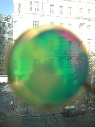
Thin-film interference is a natural phenomenon in which light waves reflected by the upper and lower boundaries of a thin film interfere with one another, increasing reflection at some wavelengths and decreasing it at others. When white light is incident on a thin film, this effect produces colorful reflections.
Crystalline silicon or (c-Si) Is the crystalline forms of silicon, either polycrystalline silicon, or monocrystalline silicon. Crystalline silicon is the dominant semiconducting material used in photovoltaic technology for the production of solar cells. These cells are assembled into solar panels as part of a photovoltaic system to generate solar power from sunlight.
Amorphous silicon (a-Si) is the non-crystalline form of silicon used for solar cells and thin-film transistors in LCDs.
Photo-reflectance is an optical technique for investigating the material and electronic properties of thin films. Photo-reflectance measures the change in reflectivity of a sample in response to the application of an amplitude modulated light beam. In general, a photo-reflectometer consists of an intensity modulated "pump" light beam used to modulate the reflectivity of the sample, a second "probe" light beam used to measure the reflectance of the sample, an optical system for directing the pump and probe beams to the sample, and for directing the reflected probe light onto a photodetector, and a signal processor to record the differential reflectance. The pump light is typically modulated at a known frequency so that a lock-in amplifier may be used to suppress unwanted noise, resulting in the ability to detect reflectance changes at the ppm level.
A rugate filter, also known as a gradient-index filter, is an optical filter based on a dielectric mirror that selectively reflects specific wavelength ranges of light. This effect is achieved by a periodic, continuous change of the refractive index of the dielectric coating. The word "rugate" is derived from corrugated structures found in nature, which also selectively reflect certain wavelength ranges of light, for example the wings of the Morpho butterfly.
The Brendel–Bormann oscillator model is a mathematical formula for the frequency dependence of the complex-valued relative permittivity, sometimes referred to as the dielectric function. The model has been used to fit to the complex refractive index of materials with absorption lineshapes exhibiting non-Lorentzian broadening, such as metals and amorphous insulators, across broad spectral ranges, typically near-ultraviolet, visible, and infrared frequencies. The dispersion relation bears the names of R. Brendel and D. Bormann, who derived the model in 1992, despite first being applied to optical constants in the literature by Andrei M. Efimov and E. G. Makarova in 1983. Around that time, several other researchers also independently discovered the model. The Brendel-Bormann oscillator model is aphysical because it does not satisfy the Kramers–Kronig relations. The model is non-causal, due to a singularity at zero frequency, and non-Hermitian. These drawbacks inspired J. Orosco and C. F. M. Coimbra to develop a similar, causal oscillator model.
The Tauc–Lorentz model is a mathematical formula for the frequency dependence of the complex-valued relative permittivity, sometimes referred to as the dielectric function. The model has been used to fit the complex refractive index of amorphous semiconductor materials at frequencies greater than their optical band gap. The dispersion relation bears the names of Jan Tauc and Hendrik Lorentz, whose previous works were combined by G. E. Jellison and F. A. Modine to create the model. The model was inspired, in part, by shortcomings of the Forouhi–Bloomer model, which is aphysical due to its incorrect asymptotic behavior and non-Hermitian character. Despite the inspiration, the Tauc–Lorentz model is itself aphysical due to being non-Hermitian and non-analytic in the upper half-plane. Further researchers have modified the model to address these shortcomings.
The Forouhi–Bloomer model is a mathematical formula for the frequency dependence of the complex-valued refractive index. The model can be used to fit the refractive index of amorphous and crystalline semiconductor and dielectric materials at energies near and greater than their optical band gap. The dispersion relation bears the names of Rahim Forouhi and Iris Bloomer, who created the model and interpreted the physical significance of its parameters. The model is aphysical due to its incorrect asymptotic behavior and non-Hermitian character. These shortcomings inspired modified versions of the model as well as development of the Tauc–Lorentz model.
1 2 Torkaman, N.M.; Ganjkhanlou, Y.; Kazemzad, M.; Dabaghi, H.H.; Keyanpour-Rad, M. (2010). "Crystallographic Parameters and Electro-Optical Constants in ITO Thin Films". Materials Characterization. 61 (3): 362–370. doi:10.1016/j.matchar.2009.12.020.
1 2 Lakhdar, M.H.; Ouni, B.; Amlouk, M. (2014). "Thickness Effect on the Structural and Optical Constants of Stibnite Thin Films Prepared by Sulfidation Annealing of Antimony Films". Optik. 125 (10): 2295–2301. Bibcode:2014Optik.125.2295L. doi:10.1016/j.ijleo.2013.10.114.
1 2 Al-Khanbashi, H.A.; Shirbeeny, W.; Al-Ghamdi, A.A.; Bronstein, L.M.; Mahmoud, W.E. (2014). "Spectroscopic Ellipsometry of Zn1−xCuxO Thin Films Based on a Modified Sol–Gel Dip-Coating Technique". Spectrochimica Acta Part A: Molecular and Biomolecular Spectroscopy. 118: 800–805. Bibcode:2014AcSpA.118..800A. doi:10.1016/j.saa.2013.09.085. PMID24157332.
1 2 Balakrishnan, G.; Sundari, S.T.; Kuppusami, P.; Chandra, P.M.; Srinivasan, M.P.; Mohandas, E.; Ganesan, V.; Sastikumar, D. (2011). "A Study of Microstructural and Optical Properties of Nanocrystalline Ceria Thin Films Prepared by Pulsed Laser Deposition". Thin Solid Films. 519 (8): 2520–2526. Bibcode:2011TSF...519.2520B. doi:10.1016/j.tsf.2010.12.013.
1 2 Cheng, K.W.; Huang, C.M.; Pan, G.T.; Chang, W.S.; Lee, T.C.; Yang, T.C.K. (2010). "Effect of Sb on the growth and photoelectrochemical response of AgIn5S8 Film Electrodes Created by Solution Growth Technique". Chemical Engineering Science. 65 (1): 74–79. doi:10.1016/j.ces.2009.02.002.
1 2 Das, N.S.; Ghosh, P.K.; Mitra, M.K.; Chattopadhyay, K.K. (2010). "Effect of Film Thickness on the Energy Band Gap of Nanocrystalline CdS Thin Films Analyzed by Spectroscopic Ellipsometry". Physica E: Low-dimensional Systems and Nanostructures. 42 (8): 2097–2102. Bibcode:2010PhyE...42.2097D. doi:10.1016/j.physe.2010.03.035.
1 2 Xiong, K.; Hou, L.; Wang, P.; Xia, Y.; Chen, D.; Xiao, B. (2014). "Phosphor-Doping Enhanced Efficiency in Bilayer Organic Solar Cells due to Longer Exciton Diffusion Length". Journal of Luminescence. 151: 193–196. Bibcode:2014JLum..151..193X. doi:10.1016/j.jlumin.2014.02.016.
1 2 Huynh, T.P.; Pietrzyk-Le, A.; Chandra-Bikram, K.C.; Noworyta, K.R.; Sobczak, J.W.; Sharma, P.S.; D'Souza, F.; Kutner, W. (2013). "Electrochemically Synthesized Molecularly Imprinted Polymer of Thiophene Derivatives for Flow-Injection Analysis Determination of Adenosine-5′-Triphosphate (ATP)". Biosensors and Bioelectronics. 41: 634–641. doi:10.1016/j.bios.2012.09.038. PMID23131778.
1 2 Zhu, D.; Shen, W.; Ye, H.; Liu, X.; Zhen, H. (2008). "Determination of the Optical Constants of Polymer Light-Emitting Diode Films from Single Reflection Measurements". Journal of Physics D: Applied Physics. 23. 41 (23): 235104. Bibcode:2008JPhD...41w5104Z. doi:10.1088/0022-3727/41/23/235104. S2CID123065042.
↑ Marquardt, D.W. (1963). "An Algorithm for Least-Squares Estimation of Nonlinear Parameters". Journal of the Society for Industrial and Applied Mathematics. 2. 11 (2): 431–441. doi:10.1137/0111030. hdl:10338.dmlcz/104299.
This page is based on this Wikipedia article Text is available under the CC BY-SA 4.0 license; additional terms may apply. Images, videos and audio are available under their respective licenses.