In CPU design, the use of a Sum Addressed Decoder (SAD) or Sum Addressed Memory (SAM) Decoder is a method of reducing the latency of the CPU cache access. This is achieved by fusing the address generation sum operation with the decode operation in the cache SRAM.
A CPU cache is a hardware cache used by the central processing unit (CPU) of a computer to reduce the average cost to access data from the main memory. A cache is a smaller, faster memory, closer to a processor core, which stores copies of the data from frequently used main memory locations. Most CPUs have different independent caches, including instruction and data caches, where the data cache is usually organized as a hierarchy of more cache levels.
The L1 data cache should usually be in the most critical CPU resource, because few things improve instructions per cycle (IPC) as directly as a larger data cache, a larger data cache takes longer to access, and pipelining the data cache makes IPC worse. One way of reducing the latency of the L1 data cache access is by fusing the address generation sum operation with the decode operation in the cache SRAM.
In computer architecture, instructions per cycle (IPC) is one aspect of a processor's performance: the average number of instructions executed for each clock cycle. It is the multiplicative inverse of cycles per instruction.
The address generation sum operation still must be performed, because other units in the memory pipe will use the resulting virtual address. That sum will be performed in parallel with the fused add/decode described here.
The most profitable recurrence to accelerate is a load, followed by a use of that load in a chain of integer operations leading to another load. Assuming that load results are bypassed with the same priority as integer results, then it's possible to summarize this recurrence as a load followed by another load—as if the program was following a linked list.
The rest of this page assumes an instruction set architecture (ISA) with a single addressing mode (register+offset), a virtually indexed data cache, and sign-extending loads that may be variable-width. Most RISC ISAs fit this description. In ISAs such as the Intelx86, three or four inputs are summed to generate the virtual address. Multiple-input additions can be reduced to a two-input addition with carry save adders, and the remaining problem is as described below. The critical recurrence, then, is an adder, a decoder, the SRAM word line, the SRAM bit line(s), the sense amp(s), the byte steering muxes, and the bypass muxes.
An instruction set architecture (ISA) is an abstract model of a computer. It is also referred to as architecture or computer architecture. A realization of an ISA is called an implementation. An ISA permits multiple implementations that may vary in performance, physical size, and monetary cost ; because the ISA serves as the interface between software and hardware. Software that has been written for an ISA can run on different implementations of the same ISA. This has enabled binary compatibility between different generations of computers to be easily achieved, and the development of computer families. Both of these developments have helped to lower the cost of computers and to increase their applicability. For these reasons, the ISA is one of the most important abstractions in computing today.
Intel Corporation is an American multinational corporation and technology company headquartered in Santa Clara, California, in the Silicon Valley. It is the world's second largest and second highest valued semiconductor chip manufacturer based on revenue after being overtaken by Samsung, and is the inventor of the x86 series of microprocessors, the processors found in most personal computers (PCs). Intel ranked No. 46 in the 2018 Fortune 500 list of the largest United States corporations by total revenue.
x86 is a family of instruction set architectures based on the Intel 8086 microprocessor and its 8088 variant. The 8086 was introduced in 1978 as a fully 16-bit extension of Intel's 8-bit 8080 microprocessor, with memory segmentation as a solution for addressing more memory than can be covered by a plain 16-bit address. The term "x86" came into being because the names of several successors to Intel's 8086 processor end in "86", including the 80186, 80286, 80386 and 80486 processors.
For this example, a direct-mapped 16KB data cache which returns doubleword (8-byte) aligned values is assumed. Each line of the SRAM is 8 bytes, and there are 2048 lines, addressed by Addr[13:3]. The sum addressed SRAM idea applies equally well to set associative caches.
The kibibyte is a multiple of the unit byte for quantities of digital information. The binary prefix kibi means 210, or 1024; therefore, 1 kibibyte is 1024 bytes. The unit symbol for the kibibyte is KiB.
Sum-addressed cache: Collapse the adder and decoder
The SRAM decoder for this example has an 11-bit input, Addr[13:3], and 2048 outputs, the decoded word lines. One word line is driven high in response to each unique Addr[13:3] value.
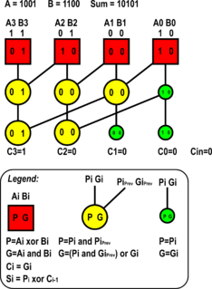
In the simplest form of decoder, each of the 2048 lines is logically an AND gate. The 11 bits (call them A[13:3] and their complements (call them B[13:3]) are driven up the decoder. For each line, 11 bits or complements are fed into an 11-input AND gate. For instance, 1026 decimal is equal to 10000000010 binary. The function for line 1026 would be:
The AND gate is a basic digital logic gate that implements logical conjunction - it behaves according to the truth table to the right. A HIGH output (1) results only if all the inputs to the AND gate are HIGH (1). If none or not all inputs to the AND gate are HIGH, a LOW output results. The function can be extended to any number of inputs.
Both the carry chain of the adder and the decoder combine information from the entire width of the index portion of the address. Combining information across the entire width twice is redundant. A sum-addressed SRAM combines the information just once by implementing the adder and decoder together in one structure.
Recall that the SRAM is indexed with the result of an add. Call the summands R (for register) and O (for the offset to that register). The sum-addressed decoder is going to decode R+O. For each decoder line, call the line number L.
Suppose that our decoder drove both R and O over each decoder line, and each decoder line implemented:
A set of full adders can be used to reduce R+O+~L to S+C (this is carry save addition). S+C==11..1 <=> S==~C. There will be no carries in the final add. Note that since C is a row of carries, it's shifted up one bit, so that R[13:3]+O[13:3]+~L[13:3] == {0,S[13:3]} + {C[14:4],0}
With this formulation, each row in the decoder is a set of full adders which reduce the base register, the offset, and the row number to a carry-save format, and a comparator. Most of this hardware will be proven redundant below, but for now it's simpler to think of it all existing in each row.
Ignoring the LSBs: Late select on carry
The formulation above checks the entire result of an add. However, in a CPU cache decoder, the entire result of the add is a byte address, and the cache is usually indexed with a larger address, in our example, that of an 8-byte block. It is preferable to ignore a few of the LSBs of the address. However, the LSBs of the two addends can't be ignored because they may produce a carry-out which would change the doubleword addressed.
If R[13:3] and O[13:3] are added to get some index I[13:3], then the actual address Addr[13:3] is equal to either I[13:3], or I[13:3] + 1, depending on whether R[2:0]+O[2:0] generates a carry-out. Both I and I+1 can be fetched if there are two banks of SRAM, one with even addresses and one with odd. The even bank holds addresses 000xxx, 010xxx, 100xxx, 110xxx, etc., and the odd bank holds addresses 001xxx, 011xxx, 101xxx, 111xxx, etc. The carry-out from R[2:0]+O[2:0] can then be used to select the even or odd doubleword fetched later.
Note that fetching from two half-size banks of SRAM will dissipate more power than fetching from one full-size bank, as it causes more switching in the sense amps and data steering logic.
Match generation
I[13:3]
even bank fetches line
odd bank fetches line
100
100
101
101
110
101
110
110
111
Referring to the adjacent diagram, the even bank will fetch line 110 when I[13:3]==101 or I[13:3]==110. The odd bank will fetch line 101 when I[13:3]==100 or I[13:3]==101.
In general, the odd SRAM bank should fetch line Lo==2N+1 when either I[13:3]==2N or I[13:3]==2N+1. The two conditions can be written as:
Ignore the last digit of the compare: (S+C)[13:4]==11..1
Similarly, the even SRAM bank fetches line Le==2N when either I[13:3]==2N or I[13:3]==2N-1. The conditions are written as follows, and once again ignore the last digit of the compare.
Before collapsing redundancy between rows, review:
Each row of each decoder for each of two banks implements a set of full adders which reduce the three numbers to be added (R[13:3], O[13:3], and L) to two numbers (S[14:4] and C[13:3]). The LSB (==S[3]) is discarded. Carry out (==C[14]) is also discarded. The row matches if S[13:4] == ~C[13:4], which is &( xor(S[13:4], C[13:4])).
It is possible to partially specialize the full adders to 2-input and, or, xor, and xnor because the L input is constant. The resulting expressions are common to all lines of the decoder and can be collected at the bottom.
S0;i = S(Ri, Oi, 0) = Ri xor Oi S1;i = S(Ri, Oi, 1) = Ri xnor Oi C0;i+1 = C(Ri, Oi, 0) = Ri and Oi C1;i+1 = C(Ri, Oi, 1) = Ri or Oi.
At each digit position, there are only two possible Si, two possible Ci, and four possible xors between them:
Li=0 and Li-1=0: X0;0;i = S0;i xor C0;i = Ri xor Oi xor (Ri-1 and Oi-1) Li=0 and Li-1=1: X0;1;i = S0;i xor C1;i = Ri xor Oi xor (Ri-1 or Oi-1) Li=1 and Li-1=0: X1;0;i = S1;i xor C0;i = Ri xnor Oi xor (Ri-1 and Oi-1) = !X0;0;i Li=1 and Li-1=1: X1;1;i = S1;i xor C1;i = Ri xnor Oi xor (Ri-1 or Oi-1) = !X0;1;i
One possible decoder for the example might calculate these four expressions for each of the bits 4..13, and drive all 40 wires up the decoder. Each line of the decoder would select one of the four wires for each bit, and consist of a 10-input AND.
What has been saved?
A simpler data cache path would have an adder followed by a traditional decoder. For our example cache subsystem, the critical path would be a 14-bit adder, producing true and complement values, followed by an 11-bit AND gate for each row of the decoder.
In the sum-addressed design, the final AND gate in the decoder remains, although 10 bits wide instead of 11. The adder has been replaced by a four input logical expression at each bit. The latency savings comes from the speed difference between the adder and that four input expression, a savings of perhaps three simple CMOS gates.
If the reader feels that this was an inordinate amount of brain-twisting work for a three gate improvement in a multi-cycle critical path, then the reader has a better appreciation for the level to which modern CPUs are optimized.
Further optimizations: predecode
Many decoder designs avoid high-fan-in AND gates in the decode line itself by employing a predecode stage. For instance, an 11-bit decoder might be predecoded into three groups of 4, 4, and 3 bits each. Each 3-bit group would drive 8 wires up the main decode array, each 4-bit group would drive 16 wires. The decoder line then becomes a 3-input AND gate. This reorganization can save significant implementation area and some power.
Fan-in is the number of inputs a logic gate can handle. For instance the fan-in for the AND gate shown in the figure is 3. Physical logic gates with a large fan-in tend to be slower than those with a small fan-in. This is because the complexity of the input circuitry increases the input capacitance of the device. Using logic gates with higher fan-in will help reducing the depth of a logic circuit.
This same reorganization can be applied to the sum-addressed decoder. Each bit in the non-predecoded formulation above can be viewed as a local two-bit add. With predecoding, each predecode group is a local three, four, or even five-bit add, with the predecode groups overlapping by one bit.
Predecoding generally increases the number of wires traversing the decoder, and sum-addressed decoders generally have about twice as many wires as the equivalent simple decoder. These wires can be the limiting factor on the amount of feasible predecoding.
Related Research Articles
Just another Perl hacker, or JAPH, typically refers to a Perl program which prints "Just another Perl hacker,". Short JAPH programs are often used as signatures in online forums, or as T-shirt designs. The phrase or acronym is also occasionally used for a signature.
In digital circuits, an adder–subtractor is a circuit that is capable of adding or subtracting numbers. Below is a circuit that does adding or subtracting depending on a control signal. It is also possible to construct a circuit that performs both addition and subtraction at the same time.
In telecommunication, a convolutional code is a type of error-correcting code that generates parity symbols via the sliding application of a boolean polynomial function to a data stream. The sliding application represents the 'convolution' of the encoder over the data, which gives rise to the term 'convolutional coding'. The sliding nature of the convolutional codes facilitates trellis decoding using a time-invariant trellis. Time invariant trellis decoding allows convolutional codes to be maximum-likelihood soft-decision decoded with reasonable complexity.
Static random-access memory is a type of semiconductor memory that uses bistable latching circuitry (flip-flop) to store each bit. SRAM exhibits data remanence, but it is still volatile in the conventional sense that data is eventually lost when the memory is not powered.
The 4000 series is a family of integrated circuits (ICs) first introduced in 1968. Almost all IC manufacturers active during this initial era fabricated models for this series. It is still in use today.
In the history of computer hardware, some early reduced instruction set computer central processing units used a very similar architectural solution, now called a classic RISC pipeline. Those CPUs were: MIPS, SPARC, Motorola 88000, and later the notional CPU DLX invented for education.
An adder is a digital circuit that performs addition of numbers. In many computers and other kinds of processors adders are used in the arithmetic logic units or ALU. They are also utilized in other parts of the processor, where they are used to calculate addresses, table indices, increment and decrement operators, and similar operations.
Transition-minimized differential signaling (TMDS), a technology for transmitting high-speed serial data, is used by the DVI and HDMI video interfaces, as well as by other digital communication interfaces.
In Boolean algebra, any Boolean function can be put into the canonical disjunctive normal form (CDNF) or minterm canonical form and its dual canonical conjunctive normal form (CCNF) or maxterm canonical form. Other canonical forms include the complete sum of prime implicants or Blake canonical form, and the algebraic normal form.
The Fredkin gate is a computational circuit suitable for reversible computing, invented by Edward Fredkin. It is universal, which means that any logical or arithmetic operation can be constructed entirely of Fredkin gates. The Fredkin gate is a circuit or device with three inputs and three outputs that transmits the first bit unchanged and swaps the last two bits if, and only if, the first bit is 1.
A carry-lookahead adder (CLA) or fast adder is a type of adder used in digital logic. A carry-look ahead adder improves speed by reducing the amount of time required to determine carry bits. It can be contrasted with the simpler, but usually slower, ripple-carry adder (RCA), for which the carry bit is calculated alongside the sum bit, and each stage must wait until the previous carry bit has been calculated to begin calculating its own sum bit and carry bit. The carry-lookahead adder calculates one or more carry bits before the sum, which reduces the wait time to calculate the result of the larger-value bits of the adder. The Kogge–Stone adder (KSA) and Brent–Kung adder (BKA) are examples of this type of adder.
A carry-skip adder is an adder implementation that improves on the delay of a ripple-carry adder with little effort compared to other adders. The improvement of the worst-case delay is achieved by using several carry-skip adders to form a block-carry-skip adder.
XOR gate is a digital logic gate that gives a true output when the number of true inputs is odd. An XOR gate implements an exclusive or; that is, a true output results if one, and only one, of the inputs to the gate is true. If both inputs are false (0/LOW) or both are true, a false output results. XOR represents the inequality function, i.e., the output is true if the inputs are not alike otherwise the output is false. A way to remember XOR is "one or the other but not both".
The R10000, code-named "T5", is a RISC microprocessor implementation of the MIPS IV instruction set architecture (ISA) developed by MIPS Technologies, Inc. (MTI), then a division of Silicon Graphics, Inc. (SGI). The chief designers are Chris Rowen and Kenneth C. Yeager. The R10000 microarchitecture is known as ANDES, an abbreviation for Architecture with Non-sequential Dynamic Execution Scheduling. The R10000 largely replaces the R8000 in the high-end and the R4400 elsewhere. MTI was a fabless semiconductor company; the R10000 was fabricated by NEC and Toshiba. Previous fabricators of MIPS microprocessors such as Integrated Device Technology (IDT) and three others did not fabricate the R10000 as it was more expensive to do so than the R4000 and R4400.
The R4000 is a microprocessor developed by MIPS Computer Systems that implements the MIPS III instruction set architecture (ISA). Officially announced on 1 October 1991, it was one of the first 64-bit microprocessors and the first MIPS III implementation. In the early 1990s, when RISC microprocessors were expected to replace CISC microprocessors such as the Intel i486, the R4000 was selected to be the microprocessor of the Advanced Computing Environment (ACE), an industry standard that intended to define a common RISC platform. ACE ultimately failed for a number of reasons, but the R4000 found success in the workstation and server markets.
The Kogge–Stone adder is a parallel prefix form carry look-ahead adder. Other parallel prefix adders (PPA) include the Brent–Kung adder (BKA), the Han–Carlson adder (HCA), and the fastest known variation, the Lynch–Swartzlander spanning tree adder (STA).
A truth table is a mathematical table used in logic—specifically in connection with Boolean algebra, boolean functions, and propositional calculus—which sets out the functional values of logical expressions on each of their functional arguments, that is, for each combination of values taken by their logical variables. In particular, truth tables can be used to show whether a propositional expression is true for all legitimate input values, that is, logically valid.
An arithmetic logic unit (ALU) is a combinational digital electronic circuit that performs arithmetic and bitwise operations on integer binary numbers. This is in contrast to a floating-point unit (FPU), which operates on floating point numbers. An ALU is a fundamental building block of many types of computing circuits, including the central processing unit (CPU) of computers, FPUs, and graphics processing units (GPUs). A single CPU, FPU or GPU may contain multiple ALUs.
The 8X300 is a microprocessor produced and marketed by Signetics starting 1976 as a second source for the SMS 300 by Scientific Micro Systems, Inc.
References
Paul Demone has an explanation of sum-addressed caches in a realworldtech article.
Heald et al.[1] have a paper in ISSCC 1998 that explains what may be the original sum-addressed cache in the Ultrasparc III.
Sum addressed memory is described in
United States patent 5,754,819, May 19, 1998, Low-latency memory indexing method and structure. Inventors: Lynch; William L. (Palo Alto, CA), Lauterbach; Gary R. (Los Altos, CA); Assignee: Sun Microsystems, Inc. (Mountain View, CA), Filed: July 28, 1994
At least one of the inventors named on a patent related to carry-free address decoding credits the following publication:
Evaluation of A + B = K Conditions without Carry Propagation (1992) Jordi Cortadella, Jose M. Llaberia IEEE Transactions on Computers,
The following patent extends this work, to use redundant form arithmetic throughout the processor, and so avoid carry propagation overhead even in ALU operations, or when an ALU operation is bypassed into a memory address:
United States Patent 5,619,664,Processor with architecture for improved pipelining of arithmetic instructions by forwarding redundant intermediate data forms, awarded April 18, 1997, Inventor: Glew; Andrew F. (Hillsboro, OR); Assignee: Intel Corporation (Santa Clara, CA), Appl. No.: 08/402,322, Filed: March 10, 1995
↑ Heald, R.; et al. (1998). "64 kB Sum-Addressed-Memory Cache with 1.6 ns Cycle and 2.6 ns Latency". ISSCC Digest of Technical Papers. pp.350–351. doi:10.1109/ISSCC.1998.672519.
This page is based on this Wikipedia article Text is available under the CC BY-SA 4.0 license; additional terms may apply. Images, videos and audio are available under their respective licenses.