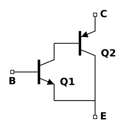
Figure 1. Sziklai pair that acts like a single NPN transistor with collector C, emitter E, and base B.
In electronics, the Sziklai pair, also known as a complementary feedback pair, is a configuration of two bipolar transistors, similar to a Darlington pair.[1] In contrast to the Darlington arrangement, the Sziklai pair has one NPN and one PNP transistor, and so it is sometimes also called the "complementary Darlington". The configuration is named for George C. Sziklai, thought to be its inventor.[2]
The current gain of the Sziklai pair is similar to that of a Darlington pair and is the product of the current gains of the two transistors. Figure 1 shows an NPN-PNP pair that acts like a single NPN transistor overall.
Applications
In a typical application the Sziklai pair acts somewhat like a single transistor with the same type (e.g., NPN) as Q1 but with a very high current gain (β). The emitter of Q2 functions as a collector. Hence the emitter of Q2 is labeled "C" in Figure 1. Likewise, in a typical application the collector of Q2 (also connected to the emitter of Q1) functions as an emitter and is thus labeled "E". As with a Darlington pair, a resistor (e.g., 100 Ω to 1 kΩ) can be connected between Q2's emitter and base to improve its turn-off time (i.e., improve its performance for high frequency signals).[1]
Advantages
One advantage over the Darlington pair is that the base turn-on voltage is only about 0.6 volts, about half of the Darlington's 1.2-volt nominal turn-on voltage.[clarification needed] Like the Darlington, it can saturate to only about 0.6 V, which is a drawback for high-power stages.
Complementary feedback-based output stages
Complementary feedback pairs are often used in the output stages of power amplifiers due to their advantages both in linearity and bandwidth when compared with more common Darlington emitter follower output stages. They are especially advantageous in amplifiers where the intended load does not require the use of parallel devices.[3][pageneeded]
Complementary feedback pairs can also have the benefit of superior thermal stability under the right conditions. In contrast to the traditional Darlington configuration, quiescent current is much more stable with respect to changes in the temperature of the higher power output transistors vs the lower power drivers.[4][circular reference][self-published source] This means that a Sziklai output stage in a class AB amplifier requires only that the bias servo transistor or diodes be thermally matched to the lower power driver transistors; they need not (and should not) be placed on the main heatsink. This potentially simplifies the design and implementation of a stable class AB amplifier, reducing the need for emitter resistors.[5][circular reference][self-published source] This significantly reduces the number of components which must be in thermal contact with the heatsink and reduces the likelihood of thermal runaway.
Optimal quiescent current in an amplifier using complementary feedback pairs also tends to be much lower than in Darlington-based output stages, on the order of 10 mA vs 100 mA or more for some emitter follower output stages. This means that idle power consumption is on the order of a few watts versus tens of watts for the same performance in many cases.[3] This is a very compelling reason to use the Sziklai pair in cases where output power is moderate (25 W to 100 W), fidelity is critical, and relatively low idle power consumption is desired.
Quasi-complementary output stages
Historically, designers frequently used the "quasi-complementary" configuration, which uses a Darlington push pair (ie, 2 NPN transistors) and a complementary feedback pull pair (ie, 1 PNP and 1 NPN transistor). This configuration, which uses 3 NPN transistors and 1 PNP transistor, was advantageous because for decades the most common small signal transistors were germanium PNPs (silicon PNP power transistors were slower to develop and were for years more expensive than their NPN counterparts). Alternately, if a germanium PNP device was used, it would have significantly different characteristics than the silicon NPN transistor. In the quasi-complementary topology, the performance of the lower pull pair, which uses a single NPN transistor, more closely matches the performance of the upper push pair, which consists of two NPN transistors and an identical power device.[4][circular reference][self-published source]
For decades the quasi-complementary output stage made sense; but because PNP and NPN power transistors are now equally available and have more closely matched performance characteristics, modern audio power amplifiers often use equivalent topologies for both pairs: either 2 Darlingtons or 2 Sziklai pairs.[4][circular reference][self-published source][5][circular reference][self-published source]
This page is based on this Wikipedia article Text is available under the CC BY-SA 4.0 license; additional terms may apply. Images, videos and audio are available under their respective licenses.