A test register, in the Intel 80386 and Intel 80486 processor, was a register used by the processor, usually to do a self-test. Most of these registers were undocumented, and used by specialized software. The test registers were named TR3 to TR7. Regular programs don't usually require these registers to work. With the Pentium, the test registers were replaced by a variety of model-specific registers (MSRs). [1]
In the 80386, two test registers, TR6 and TR7, were provided for the purpose of TLB testing. TR6 was the test command register, and TR7 was the test data register. The 80486 provided three additional registers, TR3, TR4 and TR5, for testing of the L1 cache. TR3 was a data register, TR4 was an address register and TR5 was a command register. These registers were accessed by variants of the MOV instruction. A test register may either be the source operand or the destination operand. The MOV instructions are defined in both real-address mode and protected mode. The test registers are privileged resources. In protected mode, the MOV instructions that access them can only be executed at privilege level 0. An attempt to read or write the test registers when executing at any other privilege level causes a general protection exception. Also, those instructions generate invalid opcode exception on most CPUs newer than 80486.
The instruction is encoded in two ways, depending on the flow of data. Moving data from a general purpose register into a test register is encoded as 0F 26 /r (with r/m being the GPR, and reg being the test register). Moving data the other way (i.e. from the test register into a general purpose register) is encoded as 0F 24 /r (with r/m being the GPR, and reg being the test register). [2] Only register-register moves are supported - as such, the "mod" field (top 2 bits) of the instruction's ModR/M byte should be set to 11b. (Setting the "mod" field of the ModR/M byte to anything else than 11b results in undefined behaviour, with different behaviour observed on different processors. [3] )
The test registers and/or associated opcodes were supported in the following x86 processors:
| Processors | — | Cache Test Registers | TLB Test Registers | |||||
|---|---|---|---|---|---|---|---|---|
| TR0 | TR1 | TR2 | TR3 | TR4 | TR5 | TR6 | TR7 | |
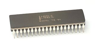
| Intel 386 (all models) | No | No | undoc [a] | Yes | ||||
| Intel 486 (all models) | No | Yes | Yes | |||||
| AMD 386 (all models) AMD Élan SC3xx | No | No | ? | Yes [5] | ||||
| AMD 486 (all models) AMD 5x86 AMD Élan SC4xx,SC5xx | No | Yes [6] | Yes | |||||
| IBM 386SLC IBM BL486SLC2/SX2/SX3 | No | Yes [7] | Yes | |||||
| C&T Super386 | No | No | Yes [8] | |||||
| NexGen Nx586 | No | No | Yes [9] | |||||
| Cyrix [b] 486 (all models [c] ) | No | Yes [11] | Yes | |||||
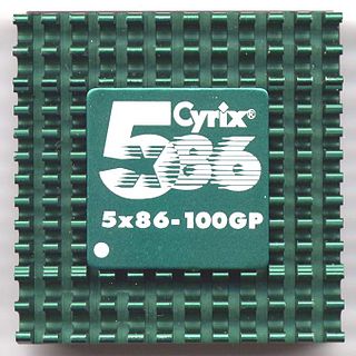
| Cyrix 5x86 | No | undoc [12] | Yes | Yes | ||||
| Cyrix 6x86 | No | undoc [d] | Yes | Yes (VSPM) [e] | ||||
| Cyrix 6x86MX, MII | No | undoc [12] | Yes (scratchpad) [f] | Yes | ||||
| VIA Cyrix III [g] | No | ? | Yes (scratchpad) [f] | Yes | ||||
| Cyrix MediaGX NatSemi Geode GX | No | ? | Yes [18] | Yes | ||||
| NatSemi Geode GX2 AMD Geode GX, LX | TR0-TR7 registers present as 32-bit read/write data registers without any cache/TLB test functionality. [19] | |||||||
| IDT WinChip (all models) | Registers not present. The MOV TRx opcodes can be enabled with the WinChip's FCR.EMOVTR [20] bit, but will act as NOPs. | |||||||
| Intel Quark X1000 | No | Yes [21] | Yes | |||||
- ↑ On the Intel 386, the TR4 and TR5 registers have been reported to act as undocumented read-only registers returning a data item related to instruction prefetch. [4]
- ↑ Cyrix manufacturing partner CPU models from IBM, TI and ST also all supported the same test registers as their corresponding Cyrix-branded CPU models.
- ↑ SoCs based on the Cyrix-derived ST486 CPU core also supported the same set of test registers as the Cyrix 486 - such SoCs include e.g. STPC Atlas and ZFMicro ZFx86. [10]
- ↑ On the Cyrix 6x86, the TR1 and TR2 registers could be enabled by setting bit 6 of Cyrix configuration register 30h. These registers are not documented, but example code using them has been published by Cyrix. [13]
- ↑ On the Cyrix 6x86, the TR6 and TR7 registers could be used not only to test the TLB, but also to configure the processor's VSPM (Variable-Size Paging Mechanism). [14] The VSPM was a 4-entry [15] software TLB with a per-entry mask to support all power-of-2 page sizes from to bytes. It was present in the Cyrix 6x86 only - it was removed in 6x86MX and later processors.
- 1 2 On the 6x86MX, MII, and "Joshua" Cyrix III processors, the TR3-TR5 registers could be used not just to test the L1 cache but also to lock individual L1 cache-lines to specific addresses for scratchpad memory use. [16] [17]
- ↑ "Joshua" core only. "Samuel" core variants of Cyrix III did not support the TRx test registers.