In processor design, microcode serves as an intermediary layer situated between the central processing unit (CPU) hardware and the programmer-visible instruction set architecture of a computer, also known as its machine code. It consists of a set of hardware-level instructions that implement the higher-level machine code instructions or control internal finite-state machine sequencing in many digital processing components. While microcode is utilized in Intel and AMD general-purpose CPUs in contemporary desktops and laptops, it functions only as a fallback path for scenarios that the faster hardwired control unit is unable to manage.

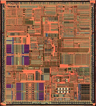
The Pentium is a microprocessor introduced by Intel on March 22, 1993. It is the first CPU using the Pentium brand. Considered the fifth generation in the x86 (8086) compatible line of processors, succeeding the i486, its implementation and microarchitecture was internally called P5.

The Pentium Pro is a sixth-generation x86 microprocessor developed and manufactured by Intel and introduced on November 1, 1995. It introduced the P6 microarchitecture and was originally intended to replace the original Pentium in a full range of applications. Later, it was reduced to a more narrow role as a server and high-end desktop processor. The Pentium Pro was also used in supercomputers, most notably ASCI Red, which used two Pentium Pro CPUs on each computing node and was the first computer to reach over one teraFLOPS in 1996, holding the number one spot in the TOP500 list from 1997 to 2000.
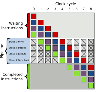
In computer engineering, instruction pipelining is a technique for implementing instruction-level parallelism within a single processor. Pipelining attempts to keep every part of the processor busy with some instruction by dividing incoming instructions into a series of sequential steps performed by different processor units with different parts of instructions processed in parallel.
In the history of computer hardware, some early reduced instruction set computer central processing units used a very similar architectural solution, now called a classic RISC pipeline. Those CPUs were: MIPS, SPARC, Motorola 88000, and later the notional CPU DLX invented for education.

In computer architecture, a branch predictor is a digital circuit that tries to guess which way a branch will go before this is known definitively. The purpose of the branch predictor is to improve the flow in the instruction pipeline. Branch predictors play a critical role in achieving high performance in many modern pipelined microprocessor architectures.
The NetBurst microarchitecture, called P68 inside Intel, was the successor to the P6 microarchitecture in the x86 family of central processing units (CPUs) made by Intel. The first CPU to use this architecture was the Willamette-core Pentium 4, released on November 20, 2000 and the first of the Pentium 4 CPUs; all subsequent Pentium 4 and Pentium D variants have also been based on NetBurst. In mid-2001, Intel released the Foster core, which was also based on NetBurst, thus switching the Xeon CPUs to the new architecture as well. Pentium 4-based Celeron CPUs also use the NetBurst architecture.
A CPU cache is a hardware cache used by the central processing unit (CPU) of a computer to reduce the average cost to access data from the main memory. A cache is a smaller, faster memory, located closer to a processor core, which stores copies of the data from frequently used main memory locations. Most CPUs have a hierarchy of multiple cache levels, with different instruction-specific and data-specific caches at level 1. The cache memory is typically implemented with static random-access memory (SRAM), in modern CPUs by far the largest part of them by chip area, but SRAM is not always used for all levels, or even any level, sometimes some latter or all levels are implemented with eDRAM.
In computer engineering, out-of-order execution is a paradigm used in high-performance central processing units to make use of instruction cycles that would otherwise be wasted. In this paradigm, a processor executes instructions in an order governed by the availability of input data and execution units, rather than by their original order in a program. In doing so, the processor can avoid being idle while waiting for the preceding instruction to complete and can, in the meantime, process the next instructions that are able to run immediately and independently.

In electronics, computer science and computer engineering, microarchitecture, also called computer organization and sometimes abbreviated as μarch or uarch, is the way a given instruction set architecture (ISA) is implemented in a particular processor. A given ISA may be implemented with different microarchitectures; implementations may vary due to different goals of a given design or due to shifts in technology.

The P6 microarchitecture is the sixth-generation Intel x86 microarchitecture, implemented by the Pentium Pro microprocessor that was introduced in November 1995. It is frequently referred to as i686. It was planned to be succeeded by the NetBurst microarchitecture used by the Pentium 4 in 2000, but was revived for the Pentium M line of microprocessors. The successor to the Pentium M variant of the P6 microarchitecture is the Core microarchitecture which in turn is also derived from P6.

In computer central processing units, micro-operations are detailed low-level instructions used in some designs to implement complex machine instructions.

Sandy Bridge is the codename for Intel's 32 nm microarchitecture used in the second generation of the Intel Core processors. The Sandy Bridge microarchitecture is the successor to Nehalem and Westmere microarchitecture. Intel demonstrated an A1 stepping Sandy Bridge processor in 2009 during Intel Developer Forum (IDF), and released first products based on the architecture in January 2011 under the Core brand.
Goldmont is a microarchitecture for low-power Atom, Celeron and Pentium branded processors used in systems on a chip (SoCs) made by Intel. They allow only one thread per core.
Goldmont Plus is a microarchitecture for low-power Celeron and Pentium Silver branded processors used in systems on a chip (SoCs) made by Intel. The Gemini Lake platform with 14 nm Goldmont Plus core was officially launched on December 11, 2017. Intel launched the Gemini Lake Refresh platform on November 4, 2019.
Intel microcode is microcode that runs inside x86 processors made by Intel. Since the P6 microarchitecture introduced in the mid-1990s, the microcode programs can be patched by the operating system or BIOS firmware to work around bugs found in the CPU after release. Intel had originally designed microcode updates for processor debugging under its design for testing (DFT) initiative.
Tremont is a microarchitecture for low-power Atom, Celeron and Pentium Silver branded processors used in systems on a chip (SoCs) made by Intel. It is the successor to Goldmont Plus. Intel officially launched Elkhart Lake platform with 10 nm Tremont core on September 23, 2020. Intel officially launched Jasper Lake platform with 10 nm Tremont core on January 11, 2021.

Golden Cove is a codename for a CPU microarchitecture developed by Intel and released in November 2021. It succeeds four microarchitectures: Sunny Cove, Skylake, Willow Cove, and Cypress Cove. It is fabricated using Intel's Intel 7 process node, previously referred to as 10 nm Enhanced SuperFin (10ESF).
Lion Cove is a 64-bit, two-way, x86 CPU core architecture designed by Intel. The Lion Cove core is featured in Core Ultra Series 2 Arrow Lake and Lunar Lake processors.


