Comparison of Intel processors

Last updated

As of 2020, the x86 architecture is used in most high end compute-intensive computers, including cloud computing, servers, workstations, and many less powerful computers, including personal computer desktops and laptops. The ARM architecture is used in most other product categories, especially high-volume battery powered mobile devices such as smartphones and tablet computers.

Contents

Some Xeon Phi processors support four-way hyper-threading, effectively quadrupling the number of threads. [1] Before the Coffee Lake architecture, most Xeon and all desktop and mobile Core i3 and i7 supported hyper-threading while only dual-core mobile i5's supported it. Post Coffee Lake, increased core counts meant hyper-threading is not needed for Core i3, as it then replaced the i5 with four physical cores on the desktop platform. Core i7, on the desktop platform no longer supports hyper-threading; instead, now higher-performing core i9s will support hyper-threading on both mobile and desktop platforms. Before 2007 and post-Kaby Lake, some Intel Pentium and Intel Atom (e.g. N270, N450) processors support hyper-threading. Celeron processors never supported it.

Intel processors table

ProcessorSeries
nomenclature
Code
name
Production dateFeatures supported (instruction set) Clock rate Socket Fabri-
cation
TDP Cores (number) Bus speed Cache L1Cache L2Cache L3 Overclock
capable
4004 N/AN/A1971 - Nov 15[ clarification needed ]N/A740 kHzDIP10-micron2N/AN/AN/A
8008 N/AN/A1972 - April good[ clarification needed ]N/A200 kHz - 800 kHzDIP10-micron1200 kHzN/AN/AN/A
8080 N/AN/A1974 - April[ clarification needed ]N/A2 MHz - 3.125 MHzDIP6-micron14 MHzN/AN/AN/A
8085 N/AN/A1976 - March[ clarification needed ]N/A3 MHz, 5 MHz, 6 MHzDIP3-micron12 MHzN/AN/AN/A
8086 N/AN/A1978 - June 15[ clarification needed ]N/A10 MHz, 8 MHz, 5 MHzDIP3-micron110 MHz, 8 MHz, 5 MHzN/AN/AN/A
8088 N/AN/A1979 - June[ clarification needed ]N/A8 MHz, 5 MHzDIP4-micron18 MHz, 5 MHzN/AN/AN/A
80286 N/AN/A1982 - Feb[ clarification needed ]N/A16 MHz, 10 MHz, 6 MHzDLPP1.9-micron122 MHz, 10 MHz, 6 MHzN/AN/AN/A
i80386 DX
SX
SL
N/A1985–1990N/A33 MHz,
25 MHz,
20 MHz,
16 MHz
DLPP1 – 1.5-micron133 MHz,
25 MHz,
20 MHz,
16 MHz
N/AN/AN/A
i80486 DX
SX
DX2
DX4
SL
N/A1989–1999N/A25 MHz – 100 MHzSocket 1
Socket 2
Socket 3
0.6 – 1-micron125 MHz – 50 MHz8 KiB – 16 KiBN/AN/A
Intel Pentium N/AP5
P54C
P54CTB
P54CS
1993–199965 MHz – 250 MHz Socket 2
Socket 3
Socket 4
Socket 5
Socket 7
350 nm – 800 nmUnknown150 MHz – 66 MHz16 KiBN/AN/A
Intel Pentium MMX N/AP55C
Tillamook
1996–1999120 MHz – 300 MHz Socket 7 250 nm – 350 nmUnknown160 MHz – 66 MHz32 KiBN/AN/A
Intel Atom Z5xx
Z6xx
N2xx
2xx
3xx
N4xx
D4xx
D5xx
N5xx
D2xxx
N2xxx
Diamondville
Pineview
Silverthorne
Lincroft
Cedarview
Medfield
Clover Trail
2008–2009 (as Centrino Atom)
2008–present (as Atom)
800 MHz – 2.13 GHzSocket PBGA437
Socket PBGA441
Socket micro-FCBGA8 559
32 nm, 45 nm0.65 W – 13 W1, 2 or 4400 MHz, 533 MHz, 667 MHz, 2.5 GT/s56 KiB per core512 KiB – 1 MiBN/A
Intel Celeron 3xx
4xx
5xx
Banias
Cedar Mill
Conroe
Coppermine
Covington
Dothan
Mendocino
Northwood
Prescott
Tualatin
Willamette
Yonah
Merom
Penryn
Arrandale
Sandy Bridge
Ivy Bridge
Haswell
Broadwell
Bay Trail-M
Braswell
Skylake
Golden Cove
1998–present266 MHz – 3.6 GHz Slot 1
Socket 370
Socket 478
Socket 479
Socket 495
LGA 775
Socket M
Socket P
FCBGA6
μFC-BGA 956
BGA479
Socket G1
BGA-1288
Socket G2
BGA-1023
Socket G3
BGA-1168
BGA-1364
BGA-1168
FC-BGA 1170
BGA 1356
LGA 1156
LGA 1155
FC-BGA 1170
LGA 1150
LGA 1151
BGA 1440
Intel 7, 14 nm, 22 nm, 32 nm, 45 nm, 65 nm, 90 nm, 130 nm, 180 nm, 250 nm4 W – 86 W1, 2 or 466 MHz, 100 MHz, 133 MHz, 400 MHz, 533 MHz, 800 MHz8 KiB – 64 KiB per core0 KiB – 1 MiB0 KiB – 2 MiB
Intel Pentium Pro 52x P6 1995–1998150 MHz – 200 MHz Socket 8 350 nm, 500 nm29.2 W – 47 W160 MHz, 66 MHz16 KiB256 KiB, 512 KiB, 1024 KiBN/A
Pentium II 52x Klamath
Deschutes
Tonga
Dixon
1997–1999233 MHz – 450 MHz Slot 1
MMC-1
MMC-2
Mini-Cartridge
250 nm, 350 nm16.8 W – 38.2 W166 MHz, 100 MHz32KiB256 KiB – 512 KiBN/A
Pentium III 52x
53x
Katmai
Coppermine
Tualatin
1999–2003450 MHz – 1.4 GHz Slot 1
Socket 370
130 nm, 180 nm, 250 nm17 W – 34.5 W1100 MHz, 133 MHz32 KiB256 KiB – 512 KiBN/A
Intel Xeon n3xxx
n5xxx
n7xxx
Allendale
Cascades
Clovertown
Conroe
Cranford
Dempsey
Drake
Dunnington
Foster
Gainestown
Gallatin
Harpertown
Irwindale
Kentsfield
Nocona
Paxville
Potomac
Prestonia
Sossaman
Tanner
Tigerton
Tulsa
Wolfdale
Woodcrest
1998–present400 MHz – 4.4 GHz Slot 2
Socket 603
Socket 604
Socket J
Socket T
Socket B
LGA 1150
LGA 1155
LGA 1156
LGA 1366
LGA 2011
LGA 2011v3
LGA 2066
Intel 7, 14 nm, 22 nm, 32 nm, 45 nm, 65 nm, 90 nm, 130 nm, 180 nm, 250 nm16 W – 165 WUp to 28 Cores (with hyperthreading)100 MHz, 133 MHz, 400 MHz, 533 MHz, 667 MHz, 800 MHz, 1066 MHz, 1333 MHz, 1600 MHz, 4.8 GT/s, 5.86 GT/s, 6.4 GT/s8 KiB ~ 64 KiB per core256 KiB – 12 MiB4 MiB – 16 MiB
Pentium 4 5xx
6xx
Cedar Mill
Northwood
Prescott
Willamette
2000–20081.3 GHz – 3.8 GHz Socket 423
Socket 478
LGA 775
Socket T
65 nm, 90 nm, 130 nm, 180 nm21 W – 115 W1 /w hyperthreading400 MHz, 533 MHz, 800 MHz, 1066 MHz8 KiB – 16 KiB256 KiB – 2 MiB2 MiB
Pentium 4 5xx
6xx
Gallatin
Prescott 2M
2000–20083.2 GHz – 3.73 GHz Socket 478
Socket T
90 nm, 130 nm92 W – 115 W1 /w hyperthreading800 MHz, 1066 MHz8 KiB512 KiB – 1 MiB0 KiB – 2 MiB
Pentium M 7xx Banias
Dothan
2003–2008800 MHz – 2.266 GHz Socket 479 90 nm, 130 nm5.5 W – 27 W1400 MHz, 533 MHz32 KiB1 MiB – 2 MiBN/A
Pentium D/EE 8xx
9xx
Smithfield
Presler
2005–20082.66 GHz – 3.73 GHz Socket T 65 nm, 90 nm95 W – 130 W2533 MHz, 800 MHz, 1066 MHz16 KiB per core2×1 MiB – 2×2 MiBN/A
Pentium Dual-Core E2xxx
E3xxx
E5xxx
T2xxx
T3xxx
Allendale
Penryn
Wolfdale
Yonah
2006–20091.6 GHz – 2.93 GHz Socket 775
Socket M
Socket P
Socket T
45 nm, 65 nm10 W – 65 W2533 MHz, 667 MHz, 800 MHz, 1066 MHz64 KiB per core1 MiB – 2 MiBN/A
Intel Pentium (2009) E2xx0
E5xxx
E6xxx
T2xxx
T3xx
T4xxx
SU2xxx
SU4xxx
G69xx
P6xxx
U5xxx
G6xx
G8xx
B9xx
G2xxx
2xxx
G3xxx
3xxx
J2xx0
J3xxx
N3xxx
G4xx0
4xxx
Penryn
Wolfdale
Clarkdale
Sandy Bridge
Ivy Bridge
Haswell
Bay Trail-D
Braswell
Skylake
Golden Cove
2009–present1.2 GHz – 3.33 GHz Socket 775
Socket P
Socket T
LGA 1156
LGA 1155
LGA 1150
LGA 1151
LGA 1200
LGA 1700
Intel 7, 14 nm, 22 nm, 32 nm, 45 nm, 65 nm2.9 W – 73 W1 or 2, 2 /w hyperthreading800 MHz, 1066 MHz, 2.5GT/s, 5 GT/s64 KiB per core2x256 KiB – 2 MiB0 KiB – 3 MiB
Intel Core Txxxx
Lxxxx
Uxxxx
Yonah 2006–20081.06 GHz – 2.33 GHz Socket M 65 nm5.5 W – 49 W1 or 2533 MHz, 667 MHz64 KiB per core2 MiBN/A
Intel Core 2 Uxxxx
Lxxxx
Exxxx
Txxxx
P7xxx
Xxxxx
Qxxxx
QXxxxx
Allendale
Conroe
Merom
Penryn
Kentsfield
Wolfdale
Yorkfield
2006–20111.06 GHz – 3.33 GHz Socket 775
Socket M
Socket P
Socket J
Socket T
45 nm, 65 nm5.5 W – 150 W1, 2 or 4533 MHz, 667 MHz, 800 MHz, 1066 MHz, 1333 MHz, 1600 MHz64 KiB per core1 MiB – 12 MiBN/A
Intel Core i3 i3-xxx
i3-2xxx
i3-3xxx
i3-4xxx
i3-61xx
i3-63xx
i3-71xx
i3-73xx
i3-81xx
i3-83xx
i3-91xx
i3-93xx
i3-101xx
i3-103xx
Arrandale
Clarkdale
Sandy Bridge
Ivy Bridge
Haswell
Skylake
Kaby Lake
Coffee Lake
Comet Lake
Golden Cove
2010–present800 MHz – 4.0 GHz LGA 1156
LGA 1155
LGA 1150
LGA 1151
LGA 1200
LGA 1700
Intel 7, 14 nm, 22 nm, 32 nm35 W – 91 W2 /w hyperthreading, 4, 4 /w hyperthreading1066 MHz, 1600 MHz, 2.5 - 5 GT/s64 KiB per core256 KiB3 MiB – 4 MiB
Intel Core i5 i5-7xx
i5-6xx
i5-2xxx
i5-3xxx
i5-4xxx
i5-5675C
i5-64xx
i5-65xx
i5-66xx
i5-74xx
i5-75xx
i5-76xx
i5-84xx
i5-85xx
i5-86xx
i5-94xx
i5-95xx
i5-96xx
i5-104xx
i5-105xx
i5-106xx
i5-114xx
i5-115xx
i5-116xx
Arrandale
Clarkdale
Clarksfield
Lynnfield
Sandy Bridge
Ivy Bridge
Haswell
Broadwell
Skylake
Kaby Lake
Coffee Lake
Comet Lake
Cypress Cove
Golden Cove
Gracemont
2009–present1.06 GHz – 4.2 GHz LGA 1156
LGA 1155
LGA 1150
LGA 1151
LGA 1200
LGA 1700
Intel 7, 14 nm, 22 nm, 32 nm, 45 nm17 W – 125 W2 - 6 /w hyperthreading,2.5 – 8 GT/s64 ~ 80 KiB per core256 ~ 512 KiB4 MiB – 12 MiB
Intel Core i7 i7-6xx
i7-7xx
i7-8xx
i7-9xx
i7-2xxx
i7-37xx
i7-38xx
i7-47xx
i7-48xx
i7-5775C
i7-58xx
i7-59xx
i7-67xx
i7-68xx
i7-69xx
i7-77xx
i7-8086K
i7-87xx
i7-97xx
i7-107xx
i7-117xx
Bloomfield
Nehalem
Clarksfield
Lynnfield
Sandy Bridge
Ivy Bridge
Haswell
Haswell Refresh, Devil‘s Canyon
Broadwell
Skylake
Kaby Lake
Coffee Lake
Comet Lake
Cypress Cove
Golden Cove
Gracemont
2008–present1.1 GHz – 4.4 GHz LGA 1156
LGA 1155
LGA 1366
LGA 2011
LGA 1150
LGA 1151
LGA 1200
LGA 1700
Intel 7, 14 nm, 22 nm, 32 nm, 45 nm35 W – 130 W4 - 6 - 8 /w hyperthreading4.8 GT/s, 8 GT/s64 ~ 80 KiB per core256 ~ 512 KiB per core6 MiB – 16 MiB
Intel Core i7 (Extreme Edition)i7-970
i7-980
i7-980x
i7-990x
i7-39xx
i7-49xx
i7-5820K
i7-59xx
i7-6800K
i7-6850K
i7-6900K
i7-6950X
(i5-7640X)
i7-7740X
i7-7820X
Gulftown
Sandy Bridge-E
Ivy Bridge-E
Haswell-E
Broadwell-E
Skylake
Kaby Lake
2011–present3.0 GHz – 5.0 GHz LGA 1366
LGA 2011
LGA 2011-v3
LGA 2066
14 nm, 22 nm, 32 nm130 W – 150 W4, 6, 8 or 10 (with hyperthreading)2.5GT/s – 8 GT/s64 KiB per core256 KiB per core12 MiB – 20 MiBYes
Intel Core i9 i9-9900K
i9-9900
i9-9900T
i9-10850K
i9-10900K
i9-10900
i9-10900T
i9-11900K
i9-11900
i9-11900T
i9-8950HK
i9-9880H
i9-9980HK
i9-10885H
i9-10980HK
Coffee Lake
Comet Lake
Cypress Cove
Golden Cove
Gracemont
2018–present3.0 GHz – 5.3 GHz LGA 1151
LGA 1200
LGA 1700
Intel 7, 14 nm35 W – 125 W6 - 8 - 10 /w hyperthreading8 GT/s64 ~ 80 KiB per core256 ~ 512 KiB per core16 MiBSome
Intel Core i9 (Extreme Edition)i9-7900X
i9-7920X
i9-7940X
i9-7960X
i9-7980XE
Kaby Lake
Cascade Lake
Q3 2017–present2.90 GHz – 4.30 GHz LGA 2066 14 nm35 W – 165 W8 - 18 (with hyperthreading)8 GT/s64 KiB per core1 MiB per core13.75 MiB – 24.75 MiBYes
ProcessorSeries
nomenclature
Code
name
Production dateFeatures supported (instruction set)Clock rateSocketFabri-
cation
TDPCores (number)Bus speedCache L1Cache L2Cache L3Overclock
capable

See also

Related Research Articles

<span class="mw-page-title-main">Celeron</span> Line of discontinued microprocessors made by Intel

Celeron is a discontinued series of low-end IA-32 and x86-64 computer microprocessor models targeted at low-cost personal computers, manufactured by Intel. The first Celeron-branded CPU was introduced on April 15, 1998, and was based on the Pentium II.

<span class="mw-page-title-main">Hyper-threading</span> Proprietary simultaneous multithreading implementation by Intel

Hyper-threading is Intel's proprietary simultaneous multithreading (SMT) implementation used to improve parallelization of computations performed on x86 microprocessors. It was introduced on Xeon server processors in February 2002 and on Pentium 4 desktop processors in November 2002. Since then, Intel has included this technology in Itanium, Atom, and Core 'i' Series CPUs, among others.

<span class="mw-page-title-main">Xeon</span> Line of Intel server and workstation processors

Xeon is a brand of x86 microprocessors designed, manufactured, and marketed by Intel, targeted at the non-consumer workstation, server, and embedded markets. It was introduced in June 1998. Xeon processors are based on the same architecture as regular desktop-grade CPUs, but have advanced features such as support for error correction code (ECC) memory, higher core counts, more PCI Express lanes, support for larger amounts of RAM, larger cache memory and extra provision for enterprise-grade reliability, availability and serviceability (RAS) features responsible for handling hardware exceptions through the Machine Check Architecture (MCA). They are often capable of safely continuing execution where a normal processor cannot due to these extra RAS features, depending on the type and severity of the machine-check exception (MCE). Some also support multi-socket systems with two, four, or eight sockets through use of the Ultra Path Interconnect (UPI) bus, which replaced the older QuickPath Interconnect (QPI) bus.

<span class="mw-page-title-main">Land grid array</span> Type of surface-mount packaging for integrated circuits

The land grid array (LGA) is a type of surface-mount packaging for integrated circuits (ICs) that is notable for having the pins on the socket — as opposed to pins on the integrated circuit, known as a pin grid array (PGA). An LGA can be electrically connected to a printed circuit board (PCB) either by the use of a socket or by soldering directly to the board.

The Intel Core microarchitecture is a multi-core processor microarchitecture launched by Intel in mid-2006. It is a major evolution over the Yonah, the previous iteration of the P6 microarchitecture series which started in 1995 with Pentium Pro. It also replaced the NetBurst microarchitecture, which suffered from high power consumption and heat intensity due to an inefficient pipeline designed for high clock rate. In early 2004 the new version of NetBurst (Prescott) needed very high power to reach the clocks it needed for competitive performance, making it unsuitable for the shift to dual/multi-core CPUs. On May 7, 2004 Intel confirmed the cancellation of the next NetBurst, Tejas and Jayhawk. Intel had been developing Merom, the 64-bit evolution of the Pentium M, since 2001, and decided to expand it to all market segments, replacing NetBurst in desktop computers and servers. It inherited from Pentium M the choice of a short and efficient pipeline, delivering superior performance despite not reaching the high clocks of NetBurst.

<span class="mw-page-title-main">Pentium</span> Brand of discontinued microprocessors produced by Intel

Pentium is a discontinued series of x86 architecture-compatible microprocessors produced by Intel. The original Pentium was first released on March 22, 1993. The name "Pentium" is originally derived from the Greek word pente (πεντε), meaning "five", a reference to the prior numeric naming convention of Intel's 80x86 processors (8086–80486), with the Latin ending -ium since the processor would otherwise have been named 80586 using that convention.

<span class="mw-page-title-main">Sandy Bridge</span> Intel processor microarchitecture

Sandy Bridge is the codename for Intel's 32 nm microarchitecture used in the second generation of the Intel Core processors. The Sandy Bridge microarchitecture is the successor to Nehalem and Westmere microarchitecture. Intel demonstrated an A1 stepping Sandy Bridge processor in 2009 during Intel Developer Forum (IDF), and released first products based on the architecture in January 2011 under the Core brand.

<span class="mw-page-title-main">Haswell (microarchitecture)</span> Intel processor microarchitecture

Haswell is the codename for a processor microarchitecture developed by Intel as the "fourth-generation core" successor to the Ivy Bridge. Intel officially announced CPUs based on this microarchitecture on June 4, 2013, at Computex Taipei 2013, while a working Haswell chip was demonstrated at the 2011 Intel Developer Forum. Haswell was the last generation of Intel processor to have socketed processors on mobile. With Haswell, which uses a 22 nm process, Intel also introduced low-power processors designed for convertible or "hybrid" ultrabooks, designated by the "U" suffix. Haswell began shipping to manufacturers and OEMs in mid-2013, with its desktop chips officially launched in September 2013.

<span class="mw-page-title-main">LGA 1156</span> Intel desktop CPU socket

LGA 1156, also known as Socket H or H1, is an Intel desktop CPU socket. Its incompatible successor is LGA 1155.

<span class="mw-page-title-main">Arrandale</span> Family of computer processors by Intel

Arrandale is the code name for a family of mobile Intel processors, sold as mobile Intel Core i3, i5 and i7 as well as Celeron and Pentium. It is closely related to the desktop Clarkdale processor; both use dual-core dies based on the Westmere 32 nm die shrink of the Nehalem microarchitecture, and have integrated Graphics as well as PCI Express and DMI links.

<span class="mw-page-title-main">Intel Core</span> Line of CPUs by Intel

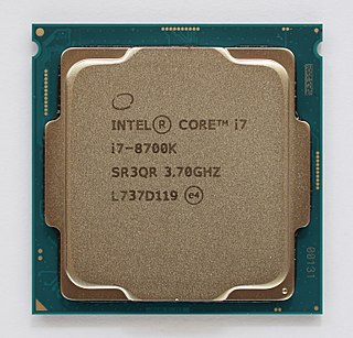
Intel Core is a line of multi-core central processing units (CPUs) for midrange, embedded, workstation, high-end and enthusiast computer markets marketed by Intel Corporation. These processors displaced the existing mid- to high-end Pentium processors at the time of their introduction, moving the Pentium to the entry level. Identical or more capable versions of Core processors are also sold as Xeon processors for the server and workstation markets.

Clarkdale is the codename for Intel's first-generation Core i5, i3 and Pentium dual-core desktop processors. It is closely related to the mobile Arrandale processor; both use dual-core dies based on the 32 nm Westmere microarchitecture and have integrated Graphics, PCI Express and DMI links built-in.

<span class="mw-page-title-main">Intel Graphics Technology</span> Series of integrated graphics processors by Intel

Intel Graphics Technology (GT) is the collective name for a series of integrated graphics processors (IGPs) produced by Intel that are manufactured on the same package or die as the central processing unit (CPU). It was first introduced in 2010 as Intel HD Graphics and renamed in 2017 as Intel UHD Graphics.

<span class="mw-page-title-main">Socket G1</span> CPU socket from Intel

Socket G1, also known as rPGA 988A, is a CPU socket introduced by Intel in 2009 for the mobile variants of the first-generation Intel Core processors. It is the successor to Socket P, and the mobile counterpart to LGA 1156 and LGA 1366.

<span class="mw-page-title-main">Broadwell (microarchitecture)</span> Fifth generation of Intel Core processors

Broadwell is the fifth generation of the Intel Core processor. It is Intel's codename for the 14 nanometer die shrink of its Haswell microarchitecture. It is a "tick" in Intel's tick–tock principle as the next step in semiconductor fabrication. Like some of the previous tick-tock iterations, Broadwell did not completely replace the full range of CPUs from the previous microarchitecture (Haswell), as there were no low-end desktop CPUs based on Broadwell.

<span class="mw-page-title-main">Kaby Lake</span> Intel microprocessor, released in 2016

Kaby Lake is Intel's codename for its seventh generation Core microprocessor family announced on August 30, 2016. Like the preceding Skylake, Kaby Lake is produced using a 14 nanometer manufacturing process technology. Breaking with Intel's previous "tick–tock" manufacturing and design model, Kaby Lake represents the optimized step of the newer process–architecture–optimization model. Kaby Lake began shipping to manufacturers and OEMs in the second quarter of 2016, with its desktop chips officially launched in January 2017.

<span class="mw-page-title-main">Coffee Lake</span> Eighth-generation Intel Core microprocessor family

Coffee Lake is Intel's codename for its eighth-generation Core microprocessor family, announced on September 25, 2017. It is manufactured using Intel's second 14 nm process node refinement. Desktop Coffee Lake processors introduced i5 and i7 CPUs featuring six cores and Core i3 CPUs with four cores and no hyperthreading.

Comet Lake is Intel's codename for its 10th generation Core processors. They are manufactured using Intel's third 14 nm Skylake process revision, succeeding the Whiskey Lake U-series mobile processor and Coffee Lake desktop processor families. Intel announced low-power mobile Comet Lake-U CPUs on August 21, 2019, H-series mobile CPUs on April 2, 2020, desktop Comet Lake-S CPUs April 30, 2020, and Xeon W-1200 series workstation CPUs on May 13, 2020. Comet Lake processors and Ice Lake 10 nm processors are together branded as the Intel "10th Generation Core" family. Intel officially launched Comet Lake-Refresh CPUs on the same day as 11th Gen Core Rocket Lake launch. The low-power mobile Comet Lake-U Core and Celeron 5205U CPUs were discontinued on July 7, 2021.

References

  1. Parallel Computing: On the Road to Exascale . Netherlands, IOS Press, 2016. 373.