
Gallium arsenide (GaAs) is a III-V direct band gap semiconductor with a zinc blende crystal structure.

Epitaxy refers to a type of crystal growth or material deposition in which new crystalline layers are formed with one or more well-defined orientations with respect to the crystalline seed layer. The deposited crystalline film is called an epitaxial film or epitaxial layer. The relative orientation(s) of the epitaxial layer to the seed layer is defined in terms of the orientation of the crystal lattice of each material. For most epitaxial growths, the new layer is usually crystalline and each crystallographic domain of the overlayer must have a well-defined orientation relative to the substrate crystal structure. Epitaxy can involve single-crystal structures, although grain-to-grain epitaxy has been observed in granular films. For most technological applications, single-domain epitaxy, which is the growth of an overlayer crystal with one well-defined orientation with respect to the substrate crystal, is preferred. Epitaxy can also play an important role while growing superlattice structures.

Cadmium sulfide is the inorganic compound with the formula CdS. Cadmium sulfide is a yellow salt. It occurs in nature with two different crystal structures as the rare minerals greenockite and hawleyite, but is more prevalent as an impurity substituent in the similarly structured zinc ores sphalerite and wurtzite, which are the major economic sources of cadmium. As a compound that is easy to isolate and purify, it is the principal source of cadmium for all commercial applications. Its vivid yellow color led to its adoption as a pigment for the yellow paint "cadmium yellow" in the 18th century.
Aluminium nitride (AlN) is a solid nitride of aluminium. It has a high thermal conductivity of up to 321 W/(m·K) and is an electrical insulator. Its wurtzite phase (w-AlN) has a band gap of ~6 eV at room temperature and has a potential application in optoelectronics operating at deep ultraviolet frequencies.
Chalcogenide glass is a glass containing one or more chalcogens. Polonium is also a chalcogen but is not used because of its strong radioactivity. Chalcogenide materials behave rather differently from oxides, in particular their lower band gaps contribute to very dissimilar optical and electrical properties.

Cadmium selenide is an inorganic compound with the formula CdSe. It is a black to red-black solid that is classified as a II-VI semiconductor of the n-type. It is a pigment, but applications are declining because of environmental concerns.
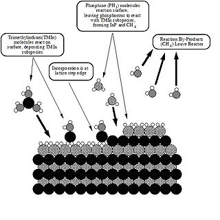
Metalorganic vapour-phase epitaxy (MOVPE), also known as organometallic vapour-phase epitaxy (OMVPE) or metalorganic chemical vapour deposition (MOCVD), is a chemical vapour deposition method used to produce single- or polycrystalline thin films. It is a process for growing crystalline layers to create complex semiconductor multilayer structures. In contrast to molecular-beam epitaxy (MBE), the growth of crystals is by chemical reaction and not physical deposition. This takes place not in vacuum, but from the gas phase at moderate pressures. As such, this technique is preferred for the formation of devices incorporating thermodynamically metastable alloys, and it has become a major process in the manufacture of optoelectronics, such as Light-emitting diodes, its most widespread application. It was first demonstrated in 1967 at North American Aviation Autonetics Division in Anaheim CA by Harold M. Manasevit.
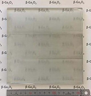
Gallium(III) oxide is an inorganic compound and ultra-wide-bandgap semiconductor with the formula Ga2O3. It is actively studied for applications in power electronics, phosphors, and gas sensing. The compound has several polymorphs, of which the monoclinic β-phase is the most stable. The β-phase’s bandgap of 4.7–4.9 eV and large-area, native substrates make it a promising competitor to GaN and SiC-based power electronics applications and solar-blind UV photodetectors. The orthorhombic ĸ-Ga2O3 is the second most stable polymorph. The ĸ-phase has shown instability of subsurface doping density under thermal exposure. Ga2O3 exhibits reduced thermal conductivity and electron mobility by an order of magnitude compared to GaN and SiC, but is predicted to be significantly more cost-effective due to being the only wide-bandgap material capable of being grown from melt. β-Ga2O3 is thought to be radiation-hard, which makes it promising for military and space applications.
Gallium(II) telluride, GaTe, is a chemical compound of gallium and tellurium. There is research interest in the structure and electronic properties of GaTe because of the possibility that it, or related compounds, may have applications in the electronics industry. Gallium telluride can be made by reacting the elements or by metal organic vapour deposition (MOCVD).
Indium(III) sulfide (Indium sesquisulfide, Indium sulfide (2:3), Indium (3+) sulfide) is the inorganic compound with the formula In2S3.

Tin selenide, also known as stannous selenide, is an inorganic compound with the formula SnSe. Tin(II) selenide is a typical layered metal chalcogenide as it includes a group 16 anion (Se2−) and an electropositive element (Sn2+), and is arranged in a layered structure. Tin(II) selenide is a narrow band-gap (IV-VI) semiconductor structurally analogous to black phosphorus. It has received considerable interest for applications including low-cost photovoltaics, and memory-switching devices.
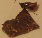
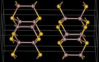
Gallium(II) selenide (GaSe) is a chemical compound. It has a hexagonal layer structure, similar to that of GaS. It is a photoconductor, a second harmonic generation crystal in nonlinear optics, and has been used as a far-infrared conversion material at 14–31 THz and above.
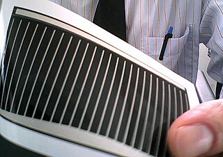
A copper indium gallium selenide solar cell is a thin-film solar cell used to convert sunlight into electric power. It is manufactured by depositing a thin layer of copper indium gallium selenide solid solution on glass or plastic backing, along with electrodes on the front and back to collect current. Because the material has a high absorption coefficient and strongly absorbs sunlight, a much thinner film is required than of other semiconductor materials.
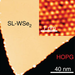
Tungsten diselenide is an inorganic compound with the formula WSe2. The compound adopts a hexagonal crystalline structure similar to molybdenum disulfide. The tungsten atoms are covalently bonded to six selenium ligands in a trigonal prismatic coordination sphere while each selenium is bonded to three tungsten atoms in a pyramidal geometry. The tungsten–selenium bond has a length of 0.2526 nm, and the distance between selenium atoms is 0.334 nm. It is a well studied example of a layered material. The layers stack together via van der Waals interactions. WSe2 is a very stable semiconductor in the group-VI transition metal dichalcogenides.

Transition-metal dichalcogenide (TMD or TMDC) monolayers are atomically thin semiconductors of the type MX2, with M a transition-metal atom (Mo, W, etc.) and X a chalcogen atom (S, Se, or Te). One layer of M atoms is sandwiched between two layers of X atoms. They are part of the large family of so-called 2D materials, named so to emphasize their extraordinary thinness. For example, a MoS2 monolayer is only 6.5 Å thick. The key feature of these materials is the interaction of large atoms in the 2D structure as compared with first-row transition-metal dichalcogenides, e.g., WTe2 exhibits anomalous giant magnetoresistance and superconductivity.
A two-dimensional semiconductor is a type of natural semiconductor with thicknesses on the atomic scale. Geim and Novoselov et al. initiated the field in 2004 when they reported a new semiconducting material graphene, a flat monolayer of carbon atoms arranged in a 2D honeycomb lattice. A 2D monolayer semiconductor is significant because it exhibits stronger piezoelectric coupling than traditionally employed bulk forms. This coupling could enable applications. One research focus is on designing nanoelectronic components by the use of graphene as electrical conductor, hexagonal boron nitride as electrical insulator, and a transition metal dichalcogenide as semiconductor.

I-III-VI2 semiconductors are solid semiconducting materials that contain three or more chemical elements belonging to groups I, III and VI (IUPAC groups 1/11, 13 and 16) of the periodic table. They usually involve two metals and one chalcogen. Some of these materials have a direct bandgap, Eg, of approximately 1.5 eV, which makes them efficient absorbers of sunlight and thus potential solar cell materials. A fourth element is often added to a I-III-VI2 material to tune the bandgap for maximum solar cell efficiency. A representative example is copper indium gallium selenide (CuInxGa(1–x)Se2, Eg = 1.7–1.0 eV for x = 0–1), which is used in copper indium gallium selenide solar cells.
Allotropes of silicon are structurally varied forms of silicon.
Selenogallates are chemical compounds which contain anionic units of selenium connected to gallium. They can be considered as gallates where selenium substitutes for oxygen. Similar compounds include the thiogallates and selenostannates. They are in the category of chalcogenotrielates or more broadly chalcogenometallates.
