Operation
The actuation process of the inchworm motor is a six step cyclical process after the initial relaxation and initialization phase. Initially, all three piezos are relaxed and unextended. To initialize the inchworm motor the clutching piezo closest to the direction of desired motion (which then becomes the forward clutch piezo) is electrified first then the six step cycle begins as follows (see Figure 2.):
Step 1. Extension of the lateral piezo.
Step 2. Extension of the aft clutch piezo.
Step 3. Relaxation of the forward clutch piezo.
Step 4. Relaxation of the lateral piezo.
Step 5. Extension of the forward clutch piezo.
Step 6. Relaxation of the aft clutch piezo.
Electrification of the piezo actuators is accomplished by applying a high bias voltage to the actuators in step according to the "Six Step" process described above. To move long distances the sequence of six steps is repeated many times in rapid succession. Once the motor has moved sufficiently close to the desired final position, the motor may be switched to an optional fine positioning mode. In this mode, the clutches receive constant voltage (one high and the other low), and the lateral piezo voltage is then adjusted to an intermediate value, under continuous feedback control, to obtain the desired final position.

A scanning tunneling microscope (STM) is a type of microscope used for imaging surfaces at the atomic level. Its development in 1981 earned its inventors, Gerd Binnig and Heinrich Rohrer, then at IBM Zürich, the Nobel Prize in Physics in 1986. STM senses the surface by using an extremely sharp conducting tip that can distinguish features smaller than 0.1 nm with a 0.01 nm depth resolution. This means that individual atoms can routinely be imaged and manipulated. Most microscopes are built for use in ultra-high vacuum at temperatures approaching zero kelvin, but variants exist for studies in air, water and other environments, and for temperatures over 1000 °C.

Atomic force microscopy (AFM) or scanning force microscopy (SFM) is a very-high-resolution type of scanning probe microscopy (SPM), with demonstrated resolution on the order of fractions of a nanometer, more than 1000 times better than the optical diffraction-limit.
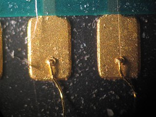
Ball bonding is a type of wire bonding, and is the most common way to make the electrical interconnections between a chip and the outside world as part of semiconductor device fabrication.
An actuator is a component of a machine that is responsible for moving and controlling a mechanism or system, for example by opening a valve. In simple terms, it is a "mover".

A piezoelectric motor or piezo motor is a type of electric motor based on the change in shape of a piezoelectric material when an electric field is applied, as a consequence of the converse piezoelectric effect. An electrical circuit makes acoustic or ultrasonic vibrations in the piezoelectric material, most often lead zirconate titanate and occasionally lithium niobate or other single-crystal materials, which can produce linear or rotary motion depending on their mechanism. Examples of types piezoelectric motors include inchworm motors, stepper and slip-stick motors as well as ultrasonic motors which can further be further categorized into standing wave and travelling wave motors.
Scanning tunneling spectroscopy (STS), an extension of scanning tunneling microscopy (STM), is used to provide information about the density of electrons in a sample as a function of their energy.

A linear actuator is an actuator that creates motion in a straight line, in contrast to the circular motion of a conventional electric motor. Linear actuators are used in machine tools and industrial machinery, in computer peripherals such as disk drives and printers, in valves and dampers, and in many other places where linear motion is required. Hydraulic or pneumatic cylinders inherently produce linear motion. Many other mechanisms are used to generate linear motion from a rotating motor.
Nanotribology is the branch of tribology that studies friction, wear, adhesion and lubrication phenomena at the nanoscale, where atomic interactions and quantum effects are not negligible. The aim of this discipline is characterizing and modifying surfaces for both scientific and technological purposes.

Scanning ion-conductance microscopy (SICM) is a scanning probe microscopy technique that uses an electrode as the probe tip. SICM allows for the determination of the surface topography of micrometer and even nanometer-range structures in aqueous media conducting electrolytes. The samples can be hard or soft, are generally non-conducting, and the non-destructive nature of the measurement allows for the observation of living tissues and cells, and biological samples in general.

Nanometrology is a subfield of metrology, concerned with the science of measurement at the nanoscale level. Nanometrology has a crucial role in order to produce nanomaterials and devices with a high degree of accuracy and reliability in nanomanufacturing.

Local oxidation nanolithography (LON) is a tip-based nanofabrication method. It is based on the spatial confinement on an oxidation reaction under the sharp tip of an atomic force microscope.
Piezoresponse force microscopy (PFM) is a variant of atomic force microscopy (AFM) that allows imaging and manipulation of piezoelectric/ferroelectric materials domains. This is achieved by bringing a sharp conductive probe into contact with a ferroelectric surface and applying an alternating current (AC) bias to the probe tip in order to excite deformation of the sample through the converse piezoelectric effect (CPE). The resulting deflection of the probe cantilever is detected through standard split photodiode detector methods and then demodulated by use of a lock-in amplifier (LiA). In this way topography and ferroelectric domains can be imaged simultaneously with high resolution.

Photoconductive atomic force microscopy (PC-AFM) is a variant of atomic force microscopy that measures photoconductivity in addition to surface forces.
The technique of vibrational analysis with scanning probe microscopy allows probing vibrational properties of materials at the submicrometer scale, and even of individual molecules. This is accomplished by integrating scanning probe microscopy (SPM) and vibrational spectroscopy. This combination allows for much higher spatial resolution than can be achieved with conventional Raman/FTIR instrumentation. The technique is also nondestructive, requires non-extensive sample preparation, and provides more contrast such as intensity contrast, polarization contrast and wavelength contrast, as well as providing specific chemical information and topography images simultaneously.
The single-molecule electric motor is an electrically operated motor made from a single butyl methyl sulphide molecule. The molecule is adsorbed onto a copper (111) single-crystal piece by chemisorption. The motor, the world's smallest electric motor, is just a nanometer across. It was developed by chemists at the Tufts University School of Arts and Sciences and published online September 4, 2011.
The Micro-Imaging Dust Analysis System (MIDAS) is one of several instruments on the European Space Agency's Rosetta mission which studied in-situ the environment around the active comet 67P/Churyumov–Gerasimenko as it flew into the inner Solar System. MIDAS is an atomic force microscope (AFM) designed to collect dust particles emitted from the comet, and then scan them with a very sharp needle-like tip to determine their 3D structure, size and texture with very high resolution.
A probe tip in scanning microscopy is a very sharp object made from metal or other materials, like a sewing needle with a point at one end with nano or sub-nanometer order of dimension. It can interact with up to one molecule or atom of a given surface of a sample that can reveal authentic properties of the surface such as morphology, topography, mapping and electrical properties of a single atom or molecule on the surface of the sample.

Multi-tip scanning tunneling microscopy extends scanning tunneling microscopy (STM) from imaging to dedicated electrical measurements at the nanoscale like a ″multimeter at the nanoscale″. In materials science, nanoscience, and nanotechnology, it is desirable to measure electrical properties at a particular position of the sample. For this purpose, multi-tip STMs in which several tips are operated independently have been developed. Apart from imaging the sample, the tips of a multi-tip STM are used to form contacts to the sample at desired locations and to perform local electrical measurements.
Nanocar Race is an international scientific competition with the aim of testing the performance of molecular machines and the scientific instruments used to control them. The race of the molecules takes place on a 100 nanometer track and was held for the first time in Toulouse on 28 and 29 April 2017.
Atomic manipulation is the process of moving single atoms on a substrate using Scanning Tunneling Microscope (STM). The atomic manipulation is a surface science technique usually used to create artificial objects on the substrate made out of atoms and to study electronic behaviour of matter. These objects do not occur in nature and therefore need to be created artificially. The first demonstration of atomic manipulation was done by IBM scientists in 1989, when they created IBM in atoms.

