Related Research Articles
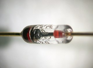
A diode is a two-terminal electronic component that conducts current primarily in one direction. It has low resistance in one direction, and high resistance in the other.
A semiconductor is a material which has an electrical conductivity value falling between that of a conductor, such as copper, and an insulator, such as glass. Its resistivity falls as its temperature rises; metals behave in the opposite way. Its conducting properties may be altered in useful ways by introducing impurities ("doping") into the crystal structure. When two differently doped regions exist in the same crystal, a semiconductor junction is created. The behavior of charge carriers, which include electrons, ions, and electron holes, at these junctions is the basis of diodes, transistors, and most modern electronics. Some examples of semiconductors are silicon, germanium, gallium arsenide, and elements near the so-called "metalloid staircase" on the periodic table. After silicon, gallium arsenide is the second-most common semiconductor and is used in laser diodes, solar cells, microwave-frequency integrated circuits, and others. Silicon is a critical element for fabricating most electronic circuits.

A transistor is a semiconductor device used to amplify or switch electrical signals and power. It is one of the basic building blocks of modern electronics. It is composed of semiconductor material, usually with at least three terminals for connection to an electronic circuit. A voltage or current applied to one pair of the transistor's terminals controls the current through another pair of terminals. Because the controlled (output) power can be higher than the controlling (input) power, a transistor can amplify a signal. Some transistors are packaged individually, but many more in miniature form are found embedded in integrated circuits. Because transistors are the key active components in practically all modern electronics, many people consider them one of the 20th century's greatest inventions.

A vacuum tube, electron tube, valve, or tube, is a device that controls electric current flow in a high vacuum between electrodes to which an electric potential difference has been applied.

A semiconductor device is an electronic component that relies on the electronic properties of a semiconductor material for its function. Its conductivity lies between conductors and insulators. Semiconductor devices have replaced vacuum tubes in most applications. They conduct electric current in the solid state, rather than as free electrons across a vacuum or as free electrons and ions through an ionized gas.

The metal-oxide-semiconductor field-effect transistor is a type of field-effect transistor (FET), most commonly fabricated by the controlled oxidation of silicon. It has an insulated gate, the voltage of which determines the conductivity of the device. This ability to change conductivity with the amount of applied voltage can be used for amplifying or switching electronic signals. A metal-insulator-semiconductor field-effect transistor (MISFET) is a term almost synonymous with MOSFET. Another synonym is IGFET for insulated-gate field-effect transistor.
A bipolar junction transistor (BJT) is a type of transistor that uses both electrons and electron holes as charge carriers. In contrast, a unipolar transistor, such as a field-effect transistor (FET), uses only one kind of charge carrier. A bipolar transistor allows a small current injected at one of its terminals to control a much larger current flowing between the terminals, making the device capable of amplification or switching.
In solid-state physics, the work function is the minimum thermodynamic work needed to remove an electron from a solid to a point in the vacuum immediately outside the solid surface. Here "immediately" means that the final electron position is far from the surface on the atomic scale, but still too close to the solid to be influenced by ambient electric fields in the vacuum. The work function is not a characteristic of a bulk material, but rather a property of the surface of the material.

A spark gap consists of an arrangement of two conducting electrodes separated by a gap usually filled with a gas such as air, designed to allow an electric spark to pass between the conductors. When the potential difference between the conductors exceeds the breakdown voltage of the gas within the gap, a spark forms, ionizing the gas and drastically reducing its electrical resistance. An electric current then flows until the path of ionized gas is broken or the current reduces below a minimum value called the "holding current". This usually happens when the voltage drops, but in some cases occurs when the heated gas rises, stretching out and then breaking the filament of ionized gas. Usually, the action of ionizing the gas is violent and disruptive, often leading to sound, light, and heat.
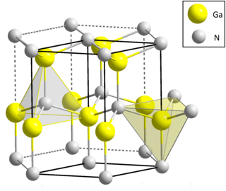
Gallium nitride is a binary III/V direct bandgap semiconductor commonly used in blue light-emitting diodes since the 1990s. The compound is a very hard material that has a Wurtzite crystal structure. Its wide band gap of 3.4 eV affords it special properties for applications in optoelectronic, high-power and high-frequency devices. For example, GaN is the substrate which makes violet (405 nm) laser diodes possible, without requiring nonlinear optical frequency-doubling.

The breakdown voltage of an insulator is the minimum voltage that causes a portion of an insulator to experience electrical breakdown and become electrically conductive.

Photodetectors, also called photosensors, are sensors of light or other electromagnetic radiation. There is a wide variety of photodetectors which may be classified by mechanism of detection, such as photoelectric or photochemical effects, or by various performance metrics, such as spectral response. Semiconductor-based photodetectors typically photo detector have a p–n junction that converts light photons into current. The absorbed photons make electron–hole pairs in the depletion region. Photodiodes and photo transistors are a few examples of photo detectors. Solar cells convert some of the light energy absorbed into electrical energy.
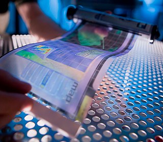
An organic field-effect transistor (OFET) is a field-effect transistor using an organic semiconductor in its channel. OFETs can be prepared either by vacuum evaporation of small molecules, by solution-casting of polymers or small molecules, or by mechanical transfer of a peeled single-crystalline organic layer onto a substrate. These devices have been developed to realize low-cost, large-area electronic products and biodegradable electronics. OFETs have been fabricated with various device geometries. The most commonly used device geometry is bottom gate with top drain and source electrodes, because this geometry is similar to the thin-film silicon transistor (TFT) using thermally grown SiO2 as gate dielectric. Organic polymers, such as poly(methyl-methacrylate) (PMMA), can also be used as dielectric. One of the benefits of OFETs, especially compared with inorganic TFTs, is their unprecedented physical flexibility, which leads to biocompatible applications, for instance in the future health care industry of personalized biomedicines and bioelectronics.

An electronic component is any basic discrete electronic device or physical entity part of an electronic system used to affect electrons or their associated fields. Electronic components are mostly industrial products, available in a singular form and are not to be confused with electrical elements, which are conceptual abstractions representing idealized electronic components and elements.

In vacuum tubes and gas-filled tubes, a hot cathode or thermionic cathode is a cathode electrode which is heated to make it emit electrons due to thermionic emission. This is in contrast to a cold cathode, which does not have a heating element. The heating element is usually an electrical filament heated by a separate electric current passing through it. Hot cathodes typically achieve much higher power density than cold cathodes, emitting significantly more electrons from the same surface area. Cold cathodes rely on field electron emission or secondary electron emission from positive ion bombardment, and do not require heating. There are two types of hot cathode. In a directly heated cathode, the filament is the cathode and emits the electrons. In an indirectly heated cathode, the filament or heater heats a separate metal cathode electrode which emits the electrons.
Hot carrier injection (HCI) is a phenomenon in solid-state electronic devices where an electron or a “hole” gains sufficient kinetic energy to overcome a potential barrier necessary to break an interface state. The term "hot" refers to the effective temperature used to model carrier density, not to the overall temperature of the device. Since the charge carriers can become trapped in the gate dielectric of a MOS transistor, the switching characteristics of the transistor can be permanently changed. Hot-carrier injection is one of the mechanisms that adversely affects the reliability of semiconductors of solid-state devices.
SONOS, short for "silicon–oxide–nitride–oxide–silicon", more precisely, "polycrystalline silicon"—"silicon dioxide"—"silicon nitride"—"silicon dioxide"—"silicon", is a cross sectional structure of MOSFET (metal–oxide–semiconductor field-effect transistor), realized by P.C.Y. Chen of Fairchild Camera and Instrument in 1977. This structure is often used for non-volatile memories, such as EEPROM and flash memories. It is sometimes used for TFT LCD displays. It is one of CTF (charge trap flash) variants. It is distinguished from traditional non-volatile memory structures by the use of silicon nitride (Si3N4 or Si9N10) instead of "polysilicon-based FG (floating-gate)" for the charge storage material. A further variant is "SHINOS" ("silicon"—"hi-k"—"nitride"—"oxide"—"silicon"), which is substituted top oxide layer with high-κ material. Another advanced variant is "MONOS" ("metal–oxide–nitride–oxide–silicon"). Companies offering SONOS-based products include Cypress Semiconductor, Macronix, Toshiba, United Microelectronics Corporation and Floadia.
In semiconductor electronics fabrication technology, a self-aligned gate is a transistor manufacturing approach whereby the gate electrode of a MOSFET is used as a mask for the doping of the source and drain regions. This technique ensures that the gate is naturally and precisely aligned to the edges of the source and drain.

A metal gate, in the context of a lateral metal–oxide–semiconductor (MOS) stack, is the gate electrode separated by an oxide from the transistor's channel – the gate material is made from a metal. In most MOS transistors since about the mid 1970s, the "M" for metal has been replaced by a non-metal gate material.

The field-effect transistor (FET) is a type of transistor that uses an electric field to control the flow of current in a semiconductor. FETs are devices with three terminals: source, gate, and drain. FETs control the flow of current by the application of a voltage to the gate, which in turn alters the conductivity between the drain and source.
References
- 1 2 3 4 Nguyen, H. (2019). "High-performance field emission based on nanostructured tin selenide for nanoscale vacuum transistors". Nanoscale. 11 (7): 3129–3137. doi:10.1039/C8NR07912A. PMID 30706919. S2CID 73445584.
- 1 2 Greene, R.; Gray, H.; Campisi, G. (1985). "Vacuum integrated circuits". 1985 International Electron Devices Meeting. Vol. 31. pp. 172–175. doi:10.1109/IEDM.1985.190922. S2CID 11778656.
- 1 2 Gray, H. F.; Campisi, G. J.; Greene, R. F. (1986). "A vacuum field effect transistor using silicon field emitter arrays". 1986 International Electron Devices Meeting. Vol. 32. pp. 776–779. doi:10.1109/IEDM.1986.191310. S2CID 26572635.
- ↑ Campisi, G. J.; Gray, H. F. (1986-01-01). "Microfabrication of Field Emission Devices for Vacuum Integrated Circuits using Orientation Dependent Etching". MRS Online Proceedings Library Archive. 76. doi:10.1557/PROC-76-67. ISSN 1946-4274.
- 1 2 Srisonphan, Siwapon; Jung, Yun Suk; Kim, Hong Koo (2012). "Metal–oxide–semiconductor field-effect transistor with a vacuum channel". Nature Nanotechnology. 7 (8): 504–508. Bibcode:2012NatNa...7..504S. doi:10.1038/nnano.2012.107. PMID 22751220.
- ↑ Han, Jin-Woo; Moon, Dong-Il; Meyyappan, M. (2017-04-12). "Nanoscale Vacuum Channel Transistor". Nano Letters. 17 (4): 2146–2151. Bibcode:2017NanoL..17.2146H. doi:10.1021/acs.nanolett.6b04363. ISSN 1530-6984. PMID 28334531. S2CID 439350.
- ↑ Shoulders, Kenneth R. (1961). Microelectronics Using Electron-Beam-Activated Machining Techniques* - ScienceDirect. pp. 135–293. doi:10.1016/S0065-2458(08)60142-4. ISBN 9780120121021.
{{cite book}}:|journal=ignored (help) - ↑ Waldrop, M. Mitchell (2016-02-11). "The chips are down for Moore's law". Nature. 530 (7589): 144–147. Bibcode:2016Natur.530..144W. doi: 10.1038/530144a . PMID 26863965.
- ↑ Sze, S. M. (1981). Physics of semiconductor devices . USA: John wiley & sons. pp. 46. ISBN 978-0-471-05661-4.
- 1 2 Han, Jin-Woo (2012-05-21). "Vacuum nanoelectronics: Back to the future?—Gate insulated nanoscale vacuum channel transistor". Applied Physics Letters. 100 (21): 213505. Bibcode:2012ApPhL.100u3505H. doi:10.1063/1.4717751. ISSN 0003-6951.