
In electrical engineering, impedance is the opposition to alternating current presented by the combined effect of resistance and reactance in a circuit.
A resistor–capacitor circuit, or RC filter or RC network, is an electric circuit composed of resistors and capacitors. It may be driven by a voltage or current source and these will produce different responses. A first order RC circuit is composed of one resistor and one capacitor and is the simplest type of RC circuit.

The Butterworth filter is a type of signal processing filter designed to have a frequency response that is as flat as possible in the passband. It is also referred to as a maximally flat magnitude filter. It was first described in 1930 by the British engineer and physicist Stephen Butterworth in his paper entitled "On the Theory of Filter Amplifiers".

An LC circuit, also called a resonant circuit, tank circuit, or tuned circuit, is an electric circuit consisting of an inductor, represented by the letter L, and a capacitor, represented by the letter C, connected together. The circuit can act as an electrical resonator, an electrical analogue of a tuning fork, storing energy oscillating at the circuit's resonant frequency.
A resistor–inductor circuit, or RL filter or RL network, is an electric circuit composed of resistors and inductors driven by a voltage or current source. A first-order RL circuit is composed of one resistor and one inductor, either in series driven by a voltage source or in parallel driven by a current source. It is one of the simplest analogue infinite impulse response electronic filters.
Foster's reactance theorem is an important theorem in the fields of electrical network analysis and synthesis. The theorem states that the reactance of a passive, lossless two-terminal (one-port) network always strictly monotonically increases with frequency. It is easily seen that the reactances of inductors and capacitors individually increase with frequency and from that basis a proof for passive lossless networks generally can be constructed. The proof of the theorem was presented by Ronald Martin Foster in 1924, although the principle had been published earlier by Foster's colleagues at American Telephone & Telegraph.
An all-pass filter is a signal processing filter that passes all frequencies equally in gain, but changes the phase relationship among various frequencies. Most types of filter reduce the amplitude of the signal applied to it for some values of frequency, whereas the all-pass filter allows all frequencies through without changes in level.

Electronic filter topology defines electronic filter circuits without taking note of the values of the components used but only the manner in which those components are connected.

Zobel networks are a type of filter section based on the image-impedance design principle. They are named after Otto Zobel of Bell Labs, who published a much-referenced paper on image filters in 1923. The distinguishing feature of Zobel networks is that the input impedance is fixed in the design independently of the transfer function. This characteristic is achieved at the expense of a much higher component count compared to other types of filter sections. The impedance would normally be specified to be constant and purely resistive. For this reason, Zobel networks are also known as constant resistance networks. However, any impedance achievable with discrete components is possible.
Image impedance is a concept used in electronic network design and analysis and most especially in filter design. The term image impedance applies to the impedance seen looking into a port of a network. Usually a two-port network is implied but the concept can be extended to networks with more than two ports. The definition of image impedance for a two-port network is the impedance, Zi 1, seen looking into port 1 when port 2 is terminated with the image impedance, Zi 2, for port 2. In general, the image impedances of ports 1 and 2 will not be equal unless the network is symmetrical with respect to the ports.

A lattice phase equaliser or lattice filter is an example of an all-pass filter. That is, the attenuation of the filter is constant at all frequencies but the relative phase between input and output varies with frequency. The lattice filter topology has the particular property of being a constant-resistance network and for this reason is often used in combination with other constant-resistance filters such as bridge-T equalisers. The topology of a lattice filter, also called an X-section, is identical to bridge topology. The lattice phase equaliser was invented by Otto Zobel using a filter topology proposed by George Campbell.
Constant k filters, also k-type filters, are a type of electronic filter designed using the image method. They are the original and simplest filters produced by this methodology and consist of a ladder network of identical sections of passive components. Historically, they are the first filters that could approach the ideal filter frequency response to within any prescribed limit with the addition of a sufficient number of sections. However, they are rarely considered for a modern design, the principles behind them having been superseded by other methodologies which are more accurate in their prediction of filter response.
m-derived filters or m-type filters are a type of electronic filter designed using the image method. They were invented by Otto Zobel in the early 1920s. This filter type was originally intended for use with telephone multiplexing and was an improvement on the existing constant k type filter. The main problem being addressed was the need to achieve a better match of the filter into the terminating impedances. In general, all filters designed by the image method fail to give an exact match, but the m-type filter is a big improvement with suitable choice of the parameter m. The m-type filter section has a further advantage in that there is a rapid transition from the cut-off frequency of the passband to a pole of attenuation just inside the stopband. Despite these advantages, there is a drawback with m-type filters; at frequencies past the pole of attenuation, the response starts to rise again, and m-types have poor stopband rejection. For this reason, filters designed using m-type sections are often designed as composite filters with a mixture of k-type and m-type sections and different values of m at different points to get the optimum performance from both types.

Prototype filters are electronic filter designs that are used as a template to produce a modified filter design for a particular application. They are an example of a nondimensionalised design from which the desired filter can be scaled or transformed. They are most often seen in regard to electronic filters and especially linear analogue passive filters. However, in principle, the method can be applied to any kind of linear filter or signal processing, including mechanical, acoustic and optical filters.
mm'-type filters, also called double-m-derived filters, are a type of electronic filter designed using the image method. They were patented by Otto Zobel in 1932. Like the m-type filter from which it is derived, the mm'-type filter type was intended to provide an improved impedance match into the filter termination impedances and originally arose in connection with telephone frequency division multiplexing. The filter has a similar transfer function to the m-type, having the same advantage of rapid cut-off, but the input impedance remains much more nearly constant if suitable parameters are chosen. In fact, the cut-off performance is better for the mm'-type if like-for-like impedance matching are compared rather than like-for-like transfer function. It also has the same drawback of a rising response in the stopband as the m-type. However, its main disadvantage is its much increased complexity which is the chief reason its use never became widespread. It was only ever intended to be used as the end sections of composite filters, the rest of the filter being made up of other sections such as k-type and m-type sections.

These filters are electrical wave filters designed using the image method. They are an invention of Otto Zobel at AT&T Corp. They are a generalisation of the m-type filter in that a transform is applied that modifies the transfer function while keeping the image impedance unchanged. For filters that have only one stopband there is no distinction with the m-type filter. However, for a filter that has multiple stopbands, there is the possibility that the form of the transfer function in each stopband can be different. For instance, it may be required to filter one band with the sharpest possible cut-off, but in another to minimise phase distortion while still achieving some attenuation. If the form is identical at each transition from passband to stopband the filter will be the same as an m-type filter. If they are different, then the general case described here pertains.

An RLC circuit is an electrical circuit consisting of a resistor (R), an inductor (L), and a capacitor (C), connected in series or in parallel. The name of the circuit is derived from the letters that are used to denote the constituent components of this circuit, where the sequence of the components may vary from RLC.
A symmetrical lattice is a two-port electrical wave filter in which diagonally-crossed shunt elements are present – a configuration which sets it apart from ladder networks. The component arrangement of the lattice is shown in the diagram below. The filter properties of this circuit were first developed using image impedance concepts, but later the more general techniques of network analysis were applied to it.
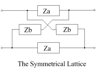
Lattice delay networks are an important subgroup of lattice networks. They are all-pass filters, so they have a flat amplitude response, but a phase response which varies linearly with frequency. All lattice circuits, regardless of their complexity, are based on the schematic shown below, which contains two series impedances, Za, and two shunt impedances, Zb. Although there is duplication of impedances in this arrangement, it offers great flexibility to the circuit designer so that, in addition to its use as delay network it can be configured to be a phase corrector, a dispersive network, an amplitude equalizer, or a low pass filter, according to the choice of components for the lattice elements.
Lattice and bridged-T equalizers are circuits which are used to correct for the amplitude and/or phase errors of a network or transmission line. Usually, the aim is to achieve an overall system performance with a flat amplitude response and constant delay over a prescribed frequency range, by the addition of an equalizer. In the past, designers have used a variety of techniques to realize their equalizer circuits. These include the method of complementary networks; the method of straight line asymptotes; using a purpose built test-jig; the use of standard circuit building blocks,; or with the aid of computer programs. In addition, trial and error methods have been found to be surprisingly effective, when performed by an experienced designer.


