
A transistor is a semiconductor device used to amplify or switch electrical signals and power. The transistor is one of the basic building blocks of modern electronics. It is composed of semiconductor material, usually with at least three terminals for connection to an electronic circuit. A voltage or current applied to one pair of the transistor's terminals controls the current through another pair of terminals. Because the controlled (output) power can be higher than the controlling (input) power, a transistor can amplify a signal. Some transistors are packaged individually, but many more are found embedded in integrated circuits.

A semiconductor device is an electronic component that relies on the electronic properties of a semiconductor material for its function. Its conductivity lies between conductors and insulators. Semiconductor devices have replaced vacuum tubes in most applications. They conduct electric current in the solid state, rather than as free electrons across a vacuum or as free electrons and ions through an ionized gas.

The metal–oxide–semiconductor field-effect transistor is a type of field-effect transistor (FET), most commonly fabricated by the controlled oxidation of silicon. It has an insulated gate, the voltage of which determines the conductivity of the device. This ability to change conductivity with the amount of applied voltage can be used for amplifying or switching electronic signals. A metal-insulator-semiconductor field-effect transistor (MISFET) is a term almost synonymous with MOSFET. Another synonym is IGFET for insulated-gate field-effect transistor.
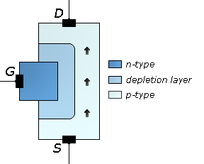
The junction-gate field-effect transistor (JFET) is one of the simplest types of field-effect transistor. JFETs are three-terminal semiconductor devices that can be used as electronically controlled switches or resistors, or to build amplifiers.
N-type metal-oxide-semiconductor logic uses n-type (-) MOSFETs to implement logic gates and other digital circuits. These nMOS transistors operate by creating an inversion layer in a p-type transistor body. This inversion layer, called the n-channel, can conduct electrons between n-type "source" and "drain" terminals. The n-channel is created by applying voltage to the third terminal, called the gate. Like other MOSFETs, nMOS transistors have four modes of operation: cut-off, triode, saturation, and velocity saturation.

Complementary metal–oxide–semiconductor is a type of metal–oxide–semiconductor field-effect transistor (MOSFET) fabrication process that uses complementary and symmetrical pairs of p-type and n-type MOSFETs for logic functions. CMOS technology is used for constructing integrated circuit (IC) chips, including microprocessors, microcontrollers, memory chips, and other digital logic circuits. CMOS technology is also used for analog circuits such as image sensors, data converters, RF circuits, and highly integrated transceivers for many types of communication.

A high-electron-mobility transistor (HEMT), also known as heterostructure FET (HFET) or modulation-doped FET (MODFET), is a field-effect transistor incorporating a junction between two materials with different band gaps as the channel instead of a doped region. A commonly used material combination is GaAs with AlGaAs, though there is wide variation, dependent on the application of the device. Devices incorporating more indium generally show better high-frequency performance, while in recent years, gallium nitride HEMTs have attracted attention due to their high-power performance. Like other FETs, HEMTs are used in integrated circuits as digital on-off switches. FETs can also be used as amplifiers for large amounts of current using a small voltage as a control signal. Both of these uses are made possible by the FET’s unique current–voltage characteristics. HEMT transistors are able to operate at higher frequencies than ordinary transistors, up to millimeter wave frequencies, and are used in high-frequency products such as cell phones, satellite television receivers, voltage converters, and radar equipment. They are widely used in satellite receivers, in low power amplifiers and in the defense industry.
In computer engineering, a logic family is one of two related concepts:
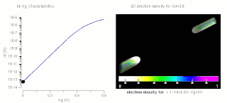
The threshold voltage, commonly abbreviated as Vth or VGS(th), of a field-effect transistor (FET) is the minimum gate-to-source voltage (VGS) that is needed to create a conducting path between the source and drain terminals. It is an important scaling factor to maintain power efficiency.

In integrated circuits, depletion-load NMOS is a form of digital logic family that uses only a single power supply voltage, unlike earlier NMOS logic families that needed more than one different power supply voltage. Although manufacturing these integrated circuits required additional processing steps, improved switching speed and the elimination of the extra power supply made this logic family the preferred choice for many microprocessors and other logic elements.
Capacitance–voltage profiling is a technique for characterizing semiconductor materials and devices. The applied voltage is varied, and the capacitance is measured and plotted as a function of voltage. The technique uses a metal–semiconductor junction or a p–n junction or a MOSFET to create a depletion region, a region which is empty of conducting electrons and holes, but may contain ionized donors and electrically active defects or traps. The depletion region with its ionized charges inside behaves like a capacitor. By varying the voltage applied to the junction it is possible to vary the depletion width. The dependence of the depletion width upon the applied voltage provides information on the semiconductor's internal characteristics, such as its doping profile and electrically active defect densities., Measurements may be done at DC, or using both DC and a small-signal AC signal, or using a large-signal transient voltage.
Negative-bias temperature instability (NBTI) is a key reliability issue in MOSFETs, a type of transistor aging. NBTI manifests as an increase in the threshold voltage and consequent decrease in drain current and transconductance of a MOSFET. The degradation is often approximated by a power-law dependence on time. It is of immediate concern in p-channel MOS devices (pMOS), since they almost always operate with negative gate-to-source voltage; however, the very same mechanism also affects nMOS transistors when biased in the accumulation regime, i.e. with a negative bias applied to the gate.
Hot carrier injection (HCI) is a phenomenon in solid-state electronic devices where an electron or a “hole” gains sufficient kinetic energy to overcome a potential barrier necessary to break an interface state. The term "hot" refers to the effective temperature used to model carrier density, not to the overall temperature of the device. Since the charge carriers can become trapped in the gate dielectric of a MOS transistor, the switching characteristics of the transistor can be permanently changed. Hot-carrier injection is one of the mechanisms that adversely affects the reliability of semiconductors of solid-state devices.
In semiconductor electronics fabrication technology, a self-aligned gate is a transistor manufacturing feature whereby the gate electrode of a MOSFET is used as a mask for the doping of the source and drain regions. This technique ensures that the gate is naturally and precisely aligned to the edges of the source and drain.

A metal gate, in the context of a lateral metal–oxide–semiconductor (MOS) stack, is the gate electrode separated by an oxide from the transistor's channel – the gate material is made from a metal. In most MOS transistors since about the mid 1970s, the "M" for metal has been replaced by a non-metal gate material.
PMOS or pMOS logic is a family of digital circuits based on p-channel, enhancement mode metal–oxide–semiconductor field-effect transistors (MOSFETs). In the late 1960s and early 1970s, PMOS logic was the dominant semiconductor technology for large-scale integrated circuits before being superseded by NMOS and CMOS devices.
The gate oxide is the dielectric layer that separates the gate terminal of a MOSFET from the underlying source and drain terminals as well as the conductive channel that connects source and drain when the transistor is turned on. Gate oxide is formed by thermal oxidation of the silicon of the channel to form a thin insulating layer of silicon dioxide. The insulating silicon dioxide layer is formed through a process of self-limiting oxidation, which is described by the Deal–Grove model. A conductive gate material is subsequently deposited over the gate oxide to form the transistor. The gate oxide serves as the dielectric layer so that the gate can sustain as high as 1 to 5 MV/cm transverse electric field in order to strongly modulate the conductance of the channel.

In field-effect transistors (FETs), depletion mode and enhancement mode are two major transistor types, corresponding to whether the transistor is in an on state or an off state at zero gate–source voltage.
Polysilicon depletion effect is the phenomenon in which unwanted variation of threshold voltage of the MOSFET devices using polysilicon as gate material is observed, leading to unpredicted behavior of the electronic circuit. Because of this variation High-k Dielectric Metal Gates (HKMG) were introduced to solve the issue.

The field-effect transistor (FET) is a type of transistor that uses an electric field to control the flow of current in a semiconductor. FETs are devices with three terminals: source, gate, and drain. FETs control the flow of current by the application of a voltage to the gate, which in turn alters the conductivity between the drain and source.