Placement (EDA)

Last updated

Placement is an essential step in electronic design automation - the portion of the physical design flow that assigns exact locations for various circuit components within the chip's core area. An inferior placement assignment will not only affect the chip's performance but might also make it nonmanufacturable by producing excessive wirelength, which is beyond available routing resources. Consequently, a placer must perform the assignment while optimizing a number of objectives to ensure that a circuit meets its performance demands.

Electronic design automation (EDA), also referred to as electronic computer-aided design (ECAD), is a category of software tools for designing electronic systems such as integrated circuits and printed circuit boards. The tools work together in a design flow that chip designers use to design and analyze entire semiconductor chips. Since a modern semiconductor chip can have billions of components, EDA tools are essential for their design.

Integrated circuit electronic circuit manufactured by lithography; set of electronic circuits on one small flat piece (or "chip") of semiconductor material, normally silicon

An integrated circuit or monolithic integrated circuit is a set of electronic circuits on one small flat piece of semiconductor material that is normally silicon. The integration of large numbers of tiny transistors into a small chip results in circuits that are orders of magnitude smaller, faster, and less expensive than those constructed of discrete electronic components. The IC's mass production capability, reliability, and building-block approach to circuit design has ensured the rapid adoption of standardized ICs in place of designs using discrete transistors. ICs are now used in virtually all electronic equipment and have revolutionized the world of electronics. Computers, mobile phones, and other digital home appliances are now inextricable parts of the structure of modern societies, made possible by the small size and low cost of ICs.

In electronic design, wire routing, commonly called simply routing, is a step in the design of printed circuit boards (PCBs) and integrated circuits (ICs). It builds on a preceding step, called placement, which determines the location of each active element of an IC or component on a PCB. After placement, the routing step adds wires needed to properly connect the placed components while obeying all design rules for the IC. Together, the placement and routing steps of IC design are known as place and route.

Contents

A placer takes a given synthesized circuit netlist together with a technology library and produces a valid placement layout. The layout is optimized according to the aforementioned objectives and ready for cell resizing and buffering — a step essential for timing and signal integrity satisfaction. Clock-tree synthesis and routing follow, completing the physical design process. In many cases, parts of, or the entire, physical design flow are iterated a number of times until design closure is achieved.

In electronic design, a netlist is a description of the connectivity of an electronic circuit. In its simplest form, a netlist consists of a list of the electronic components in a circuit and a list of the nodes they are connected to. A network (net) is a collection of two or more interconnected components.

Static timing analysis (STA) is a simulation method of computing the expected timing of a digital circuit without requiring a simulation of the full circuit.

Signal integrity

Signal integrity or SI is a set of measures of the quality of an electrical signal. In digital electronics, a stream of binary values is represented by a voltage waveform. However, digital signals are fundamentally analog in nature, and all signals are subject to effects such as noise, distortion, and loss. Over short distances and at low bit rates, a simple conductor can transmit this with sufficient fidelity. At high bit rates and over longer distances or through various mediums, various effects can degrade the electrical signal to the point where errors occur and the system or device fails. Signal integrity engineering is the task of analyzing and mitigating these effects. It is an important activity at all levels of electronics packaging and assembly, from internal connections of an integrated circuit (IC), through the package, the printed circuit board (PCB), the backplane, and inter-system connections. While there are some common themes at these various levels, there are also practical considerations, in particular the interconnect flight time versus the bit period, that cause substantial differences in the approach to signal integrity for on-chip connections versus chip-to-chip connections.

In the case of application-specific integrated circuits, or ASICs, the chip's core layout area comprises a number of fixed height rows, with either some or no space between them. Each row consists of a number of sites which can be occupied by the circuit components. A free site is a site that is not occupied by any component. Circuit components are either standard cells, macro blocks, or I/O pads. Standard cells have a fixed height equal to a row's height, but have variable widths. The width of a cell is an integral number of sites. On the other hand, blocks are typically larger than cells and have variable heights that can stretch a multiple number of rows. Some blocks can have preassigned locations — say from a previous floorplanning process — which limit the placer's task to assigning locations for just the cells. In this case, the blocks are typically referred to by fixed blocks. Alternatively, some or all of the blocks may not have preassigned locations. In this case, they have to be placed with the cells in what is commonly referred to as mixed-mode placement.

Application-specific integrated circuit Integrated circuit customized (typically optimized) for a specific task

An application-specific integrated circuit is an integrated circuit (IC) customized for a particular use, rather than intended for general-purpose use. For example, a chip designed to run in a digital voice recorder or a high-efficiency bitcoin miner is an ASIC. Application-specific standard products (ASSPs) are intermediate between ASICs and industry standard integrated circuits like the 7400 series or the 4000 series.

In addition to ASICs, placement retains its prime importance in gate array structures such as field-programmable gate arrays (FPGAs). In FPGAs, placement maps the circuit's subcircuits into programmable FPGA logic blocks in a manner that guarantees the completion of the subsequent stage of routing.

Field-programmable gate array array of logic gates that are reprogrammable

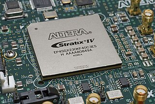
A field-programmable gate array (FPGA) is an integrated circuit designed to be configured by a customer or a designer after manufacturing – hence the term "field-programmable". The FPGA configuration is generally specified using a hardware description language (HDL), similar to that used for an Application-Specific Integrated Circuit (ASIC). Circuit diagrams were previously used to specify the configuration, but this is increasingly rare due to the advent of electronic design automation tools.

Objectives and Constraints

Placement is usually formulated as a problem of constrained optimization. The constraint is to remove overlaps between all the instances in the netlist. The optimization objective can be of multiple, which typically include:

In electronics and especially synchronous digital circuits, a clock signal is a particular type of signal that oscillates between a high and a low state and is used like a metronome to coordinate actions of digital circuits.

Basic techniques

Placement is divided into global placement and detailed placement. Global placement introduces dramatic changes by distributing all the instances to appropriate locations in the global scale with minor overlaps allowed. Detailed placement shifts each instance to nearby legal location with very moderate layout change. Placement and overall design quality is most dependent on the global placement performance.

At early time, placement of integrated circuits is handled by combinatorial approaches. When IC design was of thousand-gate scale, simulated annealing [1] methodologies such as TimberWolf [2] exhibits the best performance. As IC design entered million-scale integration, placement was achieved by recursive hyper-graph partitioning [3] like Capo. [4]

Quadratic placement later outperformed combinatorial solutions in both quality and stability. GORDIAN [5] formulates the wirelength cost as a quadratic function while still spreads cells apart through recursive partitioning. The algorithm in [6] first models placement density as a linear term into the quadratic cost function, and solves the placement problem by pure quadratic programming. Majority of the modern quadratic placers (KraftWerk, [7] FastPlace, [8] SimPL [9] ) are following this framework, each with different heuristics on how to determine the linear density force.

Nonlinear placement presents better performance over other categories of algorithms. The approach in [10] first models wirelength by exponential (nonlinear) functions and density by local piece-wise quadratic functions, in order to achieve better accuracy thus quality improvement. Follow-up academic works mainly include APlace [11] and NTUplace. [12]

ePlace [13] is the state of the art global placement algorithm. It spreads instances apart by simulating an electrostatic field, which introduces the minimum quality overhead thus achieves the best performance.

See also

The following academic journals provide further information on EDA

Related Research Articles

System on a chip type of integrated circuit

A system on a chip or system on chip is an integrated circuit that integrates all components of a computer or other electronic system. These components typically include a central processing unit (CPU), memory, input/output ports and secondary storage – all on a single substrate or microchip, the size of a coin. It may contain digital, analog, mixed-signal, and often radio frequency signal processing functions, depending on the application. As they are integrated on a single substrate, SoCs consume much less power and take up much less area than multi-chip designs with equivalent functionality. Because of this, SoCs are very common in the mobile computing and edge computing markets. Systems on chip are commonly used in embedded systems and the Internet of Things.

In numerical analysis, stochastic tunneling (STUN) is an approach to global optimization based on the Monte Carlo method-sampling of the function to be objective minimized in which the function is nonlinearly transformed to allow for easier tunneling among regions containing function minima. Easier tunneling allows for faster exploration of sample space and faster convergence to a good solution.

Place and route is a stage in the design of printed circuit boards, integrated circuits, and field-programmable gate arrays. As implied by the name, it is composed of two steps, placement and routing. The first step, placement, involves deciding where to place all electronic components, circuitry, and logic elements in a generally limited amount of space. This is followed by routing, which decides the exact design of all the wires needed to connect the placed components. This step must implement all the desired connections while following the rules and limitations of the manufacturing process.

In electronics, logic synthesis is a process by which an abstract specification of desired circuit behavior, typically at register transfer level (RTL), is turned into a design implementation in terms of logic gates, typically by a computer program called a synthesis tool. Common examples of this process include synthesis of designs specified in hardware description languages, including VHDL and Verilog. Some synthesis tools generate bitstreams for programmable logic devices such as PALs or FPGAs, while others target the creation of ASICs. Logic synthesis is one aspect of electronic design automation.

Standard cell group of transistor and interconnect structures that provides a boolean logic function; used to design application-specific integrated circuits with mostly digital-logic features

In semiconductor design, standard cell methodology is a method of designing application-specific integrated circuits (ASICs) with mostly digital-logic features. Standard cell methodology is an example of design abstraction, whereby a low-level very-large-scale integration (VLSI) layout is encapsulated into an abstract logic representation. Cell-based methodology — the general class to which standard cells belong — makes it possible for one designer to focus on the high-level aspect of digital design, while another designer focuses on the implementation (physical) aspect. Along with semiconductor manufacturing advances, standard cell methodology has helped designers scale ASICs from comparatively simple single-function ICs, to complex multi-million gate system-on-a-chip (SoC) devices.

Rent's rule pertains to the organization of computing logic, specifically the relationship between the number of external signal connections to a logic block with the number of logic gates in the logic block, and has been applied to circuits ranging from small digital circuits to mainframe computers.

Design flows are the explicit combination of electronic design automation tools to accomplish the design of an integrated circuit. Moore's law has driven the entire IC implementation RTL to GDSII design flows from one which uses primarily stand-alone synthesis, placement, and routing algorithms to an integrated construction and analysis flows for design closure. The challenges of rising interconnect delay led to a new way of thinking about and integrating design closure tools.

In VLSI semiconductor manufacturing, the process of Design Closure is a part of the development workflow by which an integrated circuit design is modified from its initial description to meet a growing list of design constraints and objectives.

Jingsheng Jason Cong is a computer scientist, educator, and serial entrepreneur. He was born in Beijing, China. He received his B.S. degree in computer science from Peking University in 1985, his M.S. and Ph. D. degrees in computer science from the University of Illinois at Urbana-Champaign in 1987 and 1990, respectively. He has been on the faculty in the Computer Science Department at the University of California, Los Angeles (UCLA) since 1990. Currently, he is a Distinguished Chancellor’s Professor and the director of Center for Domain-Specific Computing (CDSC).

Physical design (electronics)

In integrated circuit design, physical design is a step in the standard design cycle which follows after the circuit design. At this step, circuit representations of the components of the design are converted into geometric representations of shapes which, when manufactured in the corresponding layers of materials, will ensure the required functioning of the components. This geometric representation is called integrated circuit layout. This step is usually split into several sub-steps, which include both design and verification and validation of the layout.

Floorplan (microelectronics) electronic circuit schematic showing major functional blocks

In electronic design automation, a floorplan of an integrated circuit is a schematic representation of tentative placement of its major functional blocks.

In microelectronics, a three-dimensional integrated circuit is an integrated circuit manufactured by stacking silicon wafers or dies and interconnecting them vertically using, for instance, through-silicon vias (TSVs) or Cu-Cu connections, so that they behave as a single device to achieve performance improvements at reduced power and smaller footprint than conventional two dimensional processes. 3D IC is just one of a host of 3D integration schemes that exploit the z-direction to achieve electrical performance benefits.

Field-programmable gate array prototyping, also referred to as FPGA-based prototyping, ASIC prototyping or system-on-chip (SoC) prototyping, is the method to prototype system-on-chip and application-specific integrated circuit designs on FPGAs for hardware verification and early software development.

MULTICUBE is a Seventh Framework Programme (FP7) project aimed to define innovative methods for the design optimization of computer architectures for the embedded system domain.

Hardware obfuscation is a technique by which the description or the structure of electronic hardware is modified to intentionally conceal its functionality, which makes it significantly more difficult to reverse-engineer. In other words, hardware Obfuscation modifies the design in such a away that the resulting architecture becomes un-obvious to an adversary. Hardware Obfuscation can be of two types depending on the hardware platform targeted: (a) DSP Core Hardware Obfuscation - this type of obfuscation performs certain high level transformation on the data flow graph representation of DSP core to convert it into an unknown form that reflects an un-obvious architecture at RTL or gate level. This type of obfuscation is also called 'Structural Obfuscation'. Another type of DSP Core Obfuscation method is called 'Functional Obfuscation' - It uses a combination of AES and IP core locking blocks (ILBs) to lock the functionality of the DSP core using key-bits. Without application of correct key sequence, the DSP core produces either wrong output or no output at all (b) Combinational/Sequential Hardware Obfuscation - this type of obfuscation performs changes to the gate level structure of the circuit itself.

Verilog-to-Routing (VTR) is an open source CAD flow for FPGA devices. VTR's main purpose is to map a given circuit described in Verilog, a Hardware Description Language, on a given FPGA architecture for research and development purposes. The VTR project is a collaboration between the University of New Brunswick, the University of California, Berkeley and the University of Toronto. Additional contributors include Altera and Texas Instruments.

References

  1. S. Kirkpatrick, C. D. G. Jr., and M. P. Vecchi. Optimization by Simulated Annealing. Science, 220(4598):671–680, 1983.
  2. C. Sechen and A. Sangiovanni-Vincentelli. TimberWolf3.2: A New Standard Cell Placement and Global Routing Package. In DAC, pages 432–439, 1986.
  3. George Karypis, Rajat Aggarwal, Vipin Kumar, and Shashi Shekhar. Multilevel Hypergraph Partitioning: Applications in VLSI Domain. In DAC, pp. 526 - 529, 1997.
  4. Caldwell, A.E.; Kahng, A.B.; Markov, I.L. (June 2000). "Can recursive bisection alone produce routable placements? ". Proceedings of the 37th Design Automation Conference. pp. 477–482.
  5. Kleinhans, J.M.; Sigl, G.; Johannes, F.M.; Antreich, K.J. (March 1991). "GORDIAN: VLSI placement by quadratic programming and slicing optimization". IEEE Transactions on Computer-Aided Design of Integrated Circuits and Systems . 10 (3): 356–365. doi:10.1109/43.67789.
  6. H. Eisenmann and F. M. Johannes. Generic Global Placement and Floorplanning. In DAC, pages 269–274, 1998.
  7. P. Spindler, U. Schlichtmann, and F. M. Johannes. Kraftwerk2 - A Fast Force-Directed Quadratic Placement Approach Using an Accurate Net Model. IEEE TCAD, 27(8):1398–1411, 2008.
  8. N. Viswanathan, M. Pan, and C. Chu. FastPlace3.0: A Fast Multilevel Quadratic Placement Algorithm with Placement Congestion Control. In ASPDAC, pages 135–140, 2007.
  9. Kim, M.-C.; Lee D.-J.; Markov I.L. (January 2011). "SimPL: An Effective Placement Algorithm". IEEE Transactions on Computer-Aided Design of Integrated Circuits and Systems . 31 (1): 50–60. doi:10.1109/TCAD.2011.2170567.
  10. W. C. Naylor, R. Donelly, and L. Sha. Non-Linear Optimization System and Method for Wire Length and Delay Optimization for an Automatic Electric Circuit Placer. In US Patent 6301693, 2001.
  11. A. B. Kahng, S. Reda and Q. Wang, "Architecture and Details of a High Quality, Large-Scale Analytical Placer", In ICCAD 2005, pp. 891-898.
  12. T.-C. Chen, Z.-W. Jiang, T.-C. Hsu, H.-C. Chen, and Y.-W. Chang. NTUPlace3: An Analytical Placer for Large-Scale Mixed-Size Designs with Preplaced Blocks and Density Constraint. IEEE TCAD, 27(7):1228– 1240, 2008.
  13. J. Lu, P. Chen, C.-C. Chang, L. Sha, D. J.-S. Huang, C.-C. Teng and C.-K. Cheng, "ePlace: Electrostatics Based Placement Using Nesterov's Method", DAC 2014, pp. 1-6.