Chemical vapor deposition (CVD) is a vacuum deposition method used to produce high quality, high-performance, solid materials. The process is often used in the semiconductor industry to produce thin films.

Microelectromechanical systems (MEMS), also written as micro-electro-mechanical systems and the related micromechatronics and microsystems constitute the technology of microscopic devices, particularly those with moving parts. They merge at the nanoscale into nanoelectromechanical systems (NEMS) and nanotechnology. MEMS are also referred to as micromachines in Japan and microsystem technology (MST) in Europe.
Borates are boron-oxygen compounds, which form boron oxyanions. These can be trigonal or tetrahedral in structure, or more loosely can consist of chemical mixtures which contain borate anions of either description. The element boron most often occurs in nature as borates, such as borate minerals and borosilicates.

Thin-film optics is the branch of optics that deals with very thin structured layers of different materials. In order to exhibit thin-film optics, the thickness of the layers of material must be on the order of the wavelengths of visible light. Layers at this scale can have remarkable reflective properties due to light wave interference and the difference in refractive index between the layers, the air, and the substrate. These effects alter the way the optic reflects and transmits light. This effect, known as thin-film interference, is observable in soap bubbles and oil slicks.
A thin film is a layer of material ranging from fractions of a nanometer (monolayer) to several micrometers in thickness. The controlled synthesis of materials as thin films is a fundamental step in many applications. A familiar example is the household mirror, which typically has a thin metal coating on the back of a sheet of glass to form a reflective interface. The process of silvering was once commonly used to produce mirrors, while more recently the metal layer is deposited using techniques such as sputtering. Advances in thin film deposition techniques during the 20th century have enabled a wide range of technological breakthroughs in areas such as magnetic recording media, electronic semiconductor devices, Integrated passive devices, LEDs, optical coatings, hard coatings on cutting tools, and for both energy generation and storage. It is also being applied to pharmaceuticals, via thin-film drug delivery. A stack of thin films is called a multilayer.

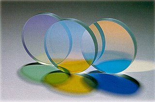
A dichroic filter, thin-film filter, or interference filter is a color filter used to selectively pass light of a small range of colors while reflecting other colors. By comparison, dichroic mirrors and dichroic reflectors tend to be characterized by the colors of light that they reflect, rather than the colors they pass.

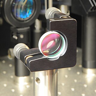
A dielectric mirror, also known as a Bragg mirror, is a type of mirror composed of multiple thin layers of dielectric material, typically deposited on a substrate of glass or some other optical material. By careful choice of the type and thickness of the dielectric layers, one can design an optical coating with specified reflectivity at different wavelengths of light. Dielectric mirrors are also used to produce ultra-high reflectivity mirrors: values of 99.999% or better over a narrow range of wavelengths can be produced using special techniques. Alternatively, they can be made to reflect a broad spectrum of light, such as the entire visible range or the spectrum of the Ti-sapphire laser. Mirrors of this type are very common in optics experiments, due to improved techniques that allow inexpensive manufacture of high-quality mirrors. Examples of their applications include laser cavity end mirrors, hot and cold mirrors, thin-film beamsplitters, high damage threshold mirrors, and the coatings on modern mirrorshades.
Cathodic arc deposition or Arc-PVD is a physical vapor deposition technique in which an electric arc is used to vaporize material from a cathode target. The vaporized material then condenses on a substrate, forming a thin film. The technique can be used to deposit metallic, ceramic, and composite films.

Ion plating (IP) is a physical vapor deposition (PVD) process that is sometimes called ion assisted deposition (IAD) or ion vapor deposition (IVD) and is a version of vacuum deposition. Ion plating uses concurrent or periodic bombardment of the substrate, and deposits film by atomic-sized energetic particles. Bombardment prior to deposition is used to sputter clean the substrate surface. During deposition the bombardment is used to modify and control the properties of the depositing film. It is important that the bombardment be continuous between the cleaning and the deposition portions of the process to maintain an atomically clean interface.

Microfabrication is a technique that use semiconductor manufacturing processes such as ion etching, diffusion, oxidation, sputtering etc. in combination with specialized micromachining techniques. This machining occurs in the range of 1-100 micrometers in size, where both the mechanical parts and the electronics that control them are built in the same piece of silicon. MEMS Fabrication consists in the application of the following steps, normally several times during the manufacturing. The process starts with a polished silicon – the substrate wafer that undergoes these steps such as Thin film growth or Deposition, Doping, Lithography and etching and Micromachining.
Atomic layer epitaxy (ALE), more generally known as atomic layer deposition (ALD), is a specialized form of thin film growth (epitaxy) that typically deposit alternating monolayers of two elements onto a substrate. The crystal lattice structure achieved is thin, uniform, and aligned with the structure of the substrate. The reactants are brought to the substrate as alternating pulses with "dead" times in between. ALE makes use of the fact that the incoming material is bound strongly until all sites available for chemisorption are occupied. The dead times are used to flush the excess material. It is mostly used in semiconductor fabrication to grow thin films of thickness in the nanometer scale.
Electron-beam physical vapor deposition, or EBPVD, is a form of physical vapor deposition in which a target anode is bombarded with an electron beam given off by a charged tungsten filament under high vacuum. The electron beam causes atoms from the target to transform into the gaseous phase. These atoms then precipitate into solid form, coating everything in the vacuum chamber with a thin layer of the anode material.

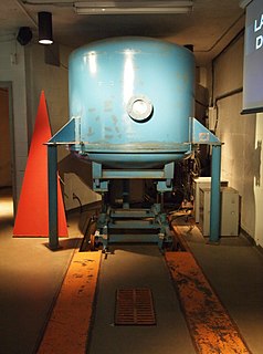
Vacuum deposition is a family of processes used to deposit layers of material atom-by-atom or molecule-by-molecule on a solid surface. These processes operate at pressures well below atmospheric pressure. The deposited layers can range from a thickness of one atom up to millimeters, forming freestanding structures. Multiple layers of different materials can be used, for example to form optical coatings. The process can be qualified based on the vapor source; physical vapor deposition uses a liquid or solid source and chemical vapor deposition uses a chemical vapor.

Physical vapor deposition (PVD), sometimes called physical vapor transport (PVT), describes a variety of vacuum deposition methods which can be used to produce thin films and coatings. PVD is characterized by a process in which the material goes from a condensed phase to a vapor phase and then back to a thin film condensed phase. The most common PVD processes are sputtering and evaporation. PVD is used in the manufacture of items which require thin films for mechanical, optical, chemical or electronic functions. Examples include semiconductor devices such as thin film solar panels, aluminized PET film for food packaging and balloons, and titanium nitride coated cutting tools for metalworking. Besides PVD tools for fabrication, special smaller tools have been developed.

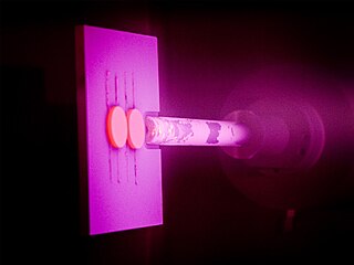
Sputter deposition is a physical vapor deposition (PVD) method of thin film deposition by sputtering. This involves ejecting material from a "target" that is a source onto a "substrate" such as a silicon wafer. Resputtering is re-emission of the deposited material during the deposition process by ion or atom bombardment. Sputtered atoms ejected from the target have a wide energy distribution, typically up to tens of eV. The sputtered ions can ballistically fly from the target in straight lines and impact energetically on the substrates or vacuum chamber. Alternatively, at higher gas pressures, the ions collide with the gas atoms that act as a moderator and move diffusively, reaching the substrates or vacuum chamber wall and condensing after undergoing a random walk. The entire range from high-energy ballistic impact to low-energy thermalized motion is accessible by changing the background gas pressure. The sputtering gas is often an inert gas such as argon. For efficient momentum transfer, the atomic weight of the sputtering gas should be close to the atomic weight of the target, so for sputtering light elements neon is preferable, while for heavy elements krypton or xenon are used. Reactive gases can also be used to sputter compounds. The compound can be formed on the target surface, in-flight or on the substrate depending on the process parameters. The availability of many parameters that control sputter deposition make it a complex process, but also allow experts a large degree of control over the growth and microstructure of the film.
Substrate is a term used in materials science and engineering to describe the base material on which processing is conducted. This surface could be used to produce new film or layers of material such as deposited coatings. It could be the base to which paint, adhesives, or adhesive tape is bonded.
The following outline is provided as an overview of and topical guide to nanotechnology:
Akhlesh Lakhtakia is Evan Pugh University Professor and Charles Godfrey Binder Professor of engineering science and mechanics at the Pennsylvania State University. His research focuses on electromagnetic fields in complex materials, such as sculptured thin films, chiral materials, bianisotropy and industrially scalable bioreplication, an emerging form of engineered biomimicry applied to harvesting of solar energy and pest eradication. His technique for visualization of latent fingerprints was covered in the NOVA documentary series "Forensics on Trial".
Stanley Shanfield serves as a Distinguished Member of the Technical Staff and Technical Director of Advanced Hardware Development at the Charles Stark Draper Laboratory in Cambridge, Massachusetts, a post he has held since 2003. He is the holder of seven patents and has led teams responsible for inventing and manufacturing new technologies in the fields of semiconductor device fabrication and optical electronics.
Valentin Borisovich Aleskovsky was a Soviet and Russian scientist and administrator known for his pioneering research on surface reactions underpinning the thin film deposition technique that years later became known as atomic layer deposition. He was the rector of Leningrad Technological Institute (1962-75) and of Leningrad State University (1975-1986).


