Shockley diode

Last updated
Shockley diode
InventedWilliam Shockley
Pin configuration  Anode and Cathode
Electronic symbol
Shockley Diode symbol.svg
A sculpture representing a Shockley 4-layer diode, on the sidewalk in front of the new building at 391 San Antonio Rd., Mountain View, California, which was the original site of the Shockley Semiconductor Laboratories where the first silicon device work in Silicon Valley was done Shockley 4-layer diode sculpture.jpg
A sculpture representing a Shockley 4-layer diode, on the sidewalk in front of the new building at 391 San Antonio Rd., Mountain View, California, which was the original site of the Shockley Semiconductor Laboratories where the first silicon device work in Silicon Valley was done

The Shockley diode (named after physicist William Shockley) is a four-layer semiconductor diode, which were one of the first semiconductor devices invented. It is a PNPN diode, with alternating layers of P-type and N-type material. It is equivalent to a thyristor with a disconnected gate. Shockley diodes were manufactured and marketed by Shockley Semiconductor Laboratory in the late 1950s. The Shockley diode has a negative resistance characteristic. [1] It was largely superseded by the diac.

Contents

Working

Diagram of a shockley diode.png
Unlike other semiconductor diodes, the Shockley diode has more than one PN junction. The construction includes four sections of semiconductors placed alternately between the anode and cathode in the pattern of PNPN. Though it has multiple junctions, it is termed a diode for being a two-terminal device.

The Shockley diode remains in an OFF state, with a very high resistance, until a voltage greater than the trigger voltage is applied across its terminals. When the voltage exceeds the trigger value, the resistance drops to an extremely low value and the device switches ON. The constituent transistors help in maintaining the ON and OFF states. As the construction resembles a pair of interconnected bipolar transistors, one PNP and other NPN, neither transistor can turn ON until the other is turned ON due to the absence of any current through the base-emitter junction. Once sufficient voltage is applied and one of the transistors breaks down, it starts conducting and allows base current to flow through the other transistor, resulting in saturation of both the transistors, keeping both in ON state.

On reducing the voltage to a sufficiently low level, the current flowing becomes insufficient to maintain the transistor bias. Due to insufficient current, one of the transistors will cut off, interrupting the base current to the other transistor, hence sealing both transistors in the OFF state.

Usages

Common applications:

Niche applications:

Typical values

V-I diagram 4capasV-I.png
V–I diagram
DescriptionRange [4] Typically
Forward operation
Switching voltage Vs10 V to 250 V50 V ± 4 V
Holding voltage Vh0.5 V to 2 V0.8 V
Switching current Isa few µA to some mA120 µA
Hold current IH1 to 50 mA14 to 45 mA
Reverse operation
Reverse current IR15 µA
Reverse breakdown voltage Vrb10 V to 250 V60 V

Dynistor

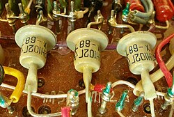
Dynistor Dinistori 2n102g.jpg
Dynistor

Small-signal Shockley diodes are no longer manufactured, but the unidirectional thyristor breakover diode, also known as the dynistor, is a functionally equivalent power device. An early publication about dynistors was published in 1958. [5] In 1988 the first dynistor using silicon carbide was made. [6] Dynistors can be used as switches in micro- and nanosecond power pulse generators. [7]

Related Research Articles

<span class="mw-page-title-main">Diode</span> Two-terminal electronic component

A diode is a two-terminal electronic component that conducts current primarily in one direction ; it has low resistance in one direction, and high resistance in the other.

<span class="mw-page-title-main">Transistor</span> Solid-state electrically operated switch also used as an amplifier

A transistor is a semiconductor device used to amplify or switch electrical signals and power. The transistor is one of the basic building blocks of modern electronics. It is composed of semiconductor material, usually with at least three terminals for connection to an electronic circuit. A voltage or current applied to one pair of the transistor's terminals controls the current through another pair of terminals. Because the controlled (output) power can be higher than the controlling (input) power, a transistor can amplify a signal. Some transistors are packaged individually, but many more in miniature form are found embedded in integrated circuits.

<span class="mw-page-title-main">Semiconductor device</span> Electronic component that exploits the electronic properties of semiconductor materials

A semiconductor device is an electronic component that relies on the electronic properties of a semiconductor material for its function. Its conductivity lies between conductors and insulators. Semiconductor devices have replaced vacuum tubes in most applications. They conduct electric current in the solid state, rather than as free electrons across a vacuum or as free electrons and ions through an ionized gas.

A unijunction transistor (UJT) is a three-lead electronic semiconductor device with only one junction that acts exclusively as an electrically controlled switch.

<span class="mw-page-title-main">Insulated-gate bipolar transistor</span> Type of solid state switch

An insulated-gate bipolar transistor (IGBT) is a three-terminal power semiconductor device primarily forming an electronic switch. It was developed to combine high efficiency with fast switching. It consists of four alternating layers (P–N–P–N) that are controlled by a metal–oxide–semiconductor (MOS) gate structure.

<span class="mw-page-title-main">Thyristor</span> Type of solid state switch

A thyristor is a solid-state semiconductor device with four layers of alternating P- and N-type materials used for high-power applications. It acts exclusively as a bistable switch, conducting when the gate receives a current trigger, and continuing to conduct until the voltage across the device is reversed biased, or until the voltage is removed. There are two designs, differing in what triggers the conducting state. In a three-lead thyristor, a small current on its Gate lead controls the larger current of the Anode to Cathode path. In a two-lead thyristor, conduction begins when the potential difference between the Anode and Cathode themselves is sufficiently large.

<span class="mw-page-title-main">Schottky diode</span> Semiconductor diode

The Schottky diode, also known as Schottky barrier diode or hot-carrier diode, is a semiconductor diode formed by the junction of a semiconductor with a metal. It has a low forward voltage drop and a very fast switching action. The cat's-whisker detectors used in the early days of wireless and metal rectifiers used in early power applications can be considered primitive Schottky diodes.

<span class="mw-page-title-main">Silicon controlled rectifier</span> Four-layer solid-state current-controlling device

A silicon controlled rectifier or semiconductor controlled rectifier is a four-layer solid-state current-controlling device. The name "silicon controlled rectifier" is General Electric's trade name for a type of thyristor. The principle of four-layer p–n–p–n switching was developed by Moll, Tanenbaum, Goldey, and Holonyak of Bell Laboratories in 1956. The practical demonstration of silicon controlled switching and detailed theoretical behavior of a device in agreement with the experimental results was presented by Dr Ian M. Mackintosh of Bell Laboratories in January 1958. The SCR was developed by a team of power engineers led by Gordon Hall and commercialized by Frank W. "Bill" Gutzwiller in 1957.

<span class="mw-page-title-main">TRIAC</span> Solid-state semiconductor device

A TRIAC is a three terminal electronic component that conducts current in either direction when triggered. The term TRIAC is a genericised trademark.

<span class="mw-page-title-main">DIAC</span>

The DIAC is a diode that conducts electrical current only after its breakover voltage, VBO, has been reached momentarily. Three, four, and five layer structures may be used. Behavior is similar to the voltage breakdown of a triac without a gate terminal.

<span class="mw-page-title-main">Tunnel diode</span> Diode that works using quantum tunneling effect

A tunnel diode or Esaki diode is a type of semiconductor diode that has effectively "negative resistance" due to the quantum mechanical effect called tunneling. It was invented in August 1957 by Leo Esaki, Yuriko Kurose, and Takashi Suzuki when they were working at Tokyo Tsushin Kogyo, now known as Sony. In 1973, Esaki received the Nobel Prize in Physics, jointly with Brian Josephson, for discovering the electron tunneling effect used in these diodes. Robert Noyce independently devised the idea of a tunnel diode while working for William Shockley, but was discouraged from pursuing it. Tunnel diodes were first manufactured by Sony in 1957, followed by General Electric and other companies from about 1960, and are still made in low volume today.

A power semiconductor device is a semiconductor device used as a switch or rectifier in power electronics. Such a device is also called a power device or, when used in an integrated circuit, a power IC.

<span class="mw-page-title-main">Electronic component</span> Discrete device in an electronic system

An electronic component is any basic discrete device or physical entity in an electronic system used to affect electrons or their associated fields. Electronic components are mostly industrial products, available in a singular form and are not to be confused with electrical elements, which are conceptual abstractions representing idealized electronic components and elements.

<span class="mw-page-title-main">Power MOSFET</span> MOSFET that can handle significant power levels

A power MOSFET is a specific type of metal–oxide–semiconductor field-effect transistor (MOSFET) designed to handle significant power levels. Compared to the other power semiconductor devices, such as an insulated-gate bipolar transistor (IGBT) or a thyristor, its main advantages are high switching speed and good efficiency at low voltages. It shares with the IGBT an isolated gate that makes it easy to drive. They can be subject to low gain, sometimes to a degree that the gate voltage needs to be higher than the voltage under control.

An avalanche transistor is a bipolar junction transistor designed for operation in the region of its collector-current/collector-to-emitter voltage characteristics beyond the collector-to-emitter breakdown voltage, called avalanche breakdown region. This region is characterized by avalanche breakdown, which is a phenomenon similar to Townsend discharge for gases, and negative differential resistance. Operation in the avalanche breakdown region is called avalanche-mode operation: it gives avalanche transistors the ability to switch very high currents with less than a nanosecond rise and fall times. Transistors not specifically designed for the purpose can have reasonably consistent avalanche properties; for example 82% of samples of the 15V high-speed switch 2N2369, manufactured over a 12-year period, were capable of generating avalanche breakdown pulses with rise time of 350 ps or less, using a 90V power supply as Jim Williams writes.

<span class="mw-page-title-main">Gate turn-off thyristor</span>

A gate turn-off thyristor (GTO) is a special type of thyristor, which is a high-power semiconductor device. It was invented by General Electric. GTOs, as opposed to normal thyristors, are fully controllable switches which can be turned on and off by their gate lead.

A QUADRAC is a special type of thyristor which combines a DIAC and a TRIAC in a single package. The DIAC is the triggering device for the TRIAC. Thyristors are four-layer (PNPN) semiconductor devices that act as switches, rectifiers or voltage regulators in a variety of applications. When triggered, thyristors turn on and become low-resistance current paths. They remain so even after the trigger is removed, and until the current is reduced to a certain level. Diacs are bi-directional diodes that switch AC voltages and trigger triacs or silicon-controlled rectifiers (SCRs). Except for a small leakage current, diacs do not conduct until the breakover voltage is reached. Triacs are three-terminal, silicon devices that function as two SCRs configured in an inverse, parallel arrangement. They provide load current during both halves of the AC supply voltage. By combining the functions of diacs and triacs, QUADRACs eliminate the need to buy and assemble discrete parts.

The following outline is provided as an overview of and topical guide to electronics:

<span class="mw-page-title-main">Field-effect transistor</span> Type of transistor

The field-effect transistor (FET) is a type of transistor that uses an electric field to control the flow of current in a semiconductor. FETs are devices with three terminals: source, gate, and drain. FETs control the flow of current by the application of a voltage to the gate, which in turn alters the conductivity between the drain and source.

<span class="mw-page-title-main">Igor Grekhov</span>

Igor Vsevolodovich Grekhov is a Soviet and Russian physicist and electrical engineer, full member of the Russian Academy of Sciences. He is known as one of the founders of the power semiconductor device industry in the Soviet Union. His contributions to the field of pulsed power devices and converter technique were recognized by the awarding of the Lenin Prize, the two State Prizes and several State orders of Russia. He headed the laboratory at the Ioffe Physical Technical Institute in St. Petersburg over several decades.

References

  1. "Transistor Museum Photo Gallery Shockley Diode 4 LayerTransistor". semiconductormuseum.com. Retrieved 2019-04-09.
  2. "Transistor Museum Photo Gallery Shockley Diode Transistor 4 Layer". semiconductormuseum.com. Retrieved 2019-04-09.
  3. "Just Diodes In Hi-Fi Amplifier". 2007-02-21. Archived from the original on 2007-02-21. Retrieved 2019-04-09.
  4. Willfried Schurig (1971), amateurreihe electronica: Kennlinien elektronischer Bauelemente. Teil II: Halbleiter Dioden (in German), Berlin: Deutscher Militärverlag, p. 119
  5. Pittman, P. (Spring 1958). The application of the dynistor diode to off-on controllers. 1958 IEEE International Solid-State Circuits Conference. Digest of Technical Papers. Vol. I. pp. 55–56. doi:10.1109/ISSCC.1958.1155602.
  6. Chelnokov, V. E.; Vainshtein, S. N.; Levinshtein, M. E.; Dmitriev, V. A. (1988-08-04). "First SiC dynistor". Electronics Letters. 24 (16): 1031–1033. doi:10.1049/el:19880702. ISSN   1350-911X.
  7. Aristov, Yu.V.; Grekhov, I.V.; Korotkov, S.V.; Lyublinsky, A.G. (September 22–26, 2008). "Dynistor Switches for Micro- and Nanosecond Power Pulse Generators". Acta Physica Polonica A. Proceedings of the 2nd Euro-Asian Pulsed Power Conference, Vilnius, Lithuania, September 22–26, 2008. 115 (6): 1031–1033. doi: 10.12693/APhysPolA.115.1031 .