An electron microscope is a microscope that uses a beam of electrons as a source of illumination. They use electron optics that are analogous to the glass lenses of an optical light microscope to control the electron beam, for instance focusing them to produce magnified images or electron diffraction patterns. As the wavelength of an electron can be up to 100,000 times smaller than that of visible light, electron microscopes have a much higher resolution of about 0.1 nm, which compares to about 200 nm for light microscopes. Electron microscope may refer to:

Microscopy is the technical field of using microscopes to view objects and areas of objects that cannot be seen with the naked eye. There are three well-known branches of microscopy: optical, electron, and scanning probe microscopy, along with the emerging field of X-ray microscopy.

A scanning electron microscope (SEM) is a type of electron microscope that produces images of a sample by scanning the surface with a focused beam of electrons. The electrons interact with atoms in the sample, producing various signals that contain information about the surface topography and composition of the sample. The electron beam is scanned in a raster scan pattern, and the position of the beam is combined with the intensity of the detected signal to produce an image. In the most common SEM mode, secondary electrons emitted by atoms excited by the electron beam are detected using a secondary electron detector. The number of secondary electrons that can be detected, and thus the signal intensity, depends, among other things, on specimen topography. Some SEMs can achieve resolutions better than 1 nanometer.

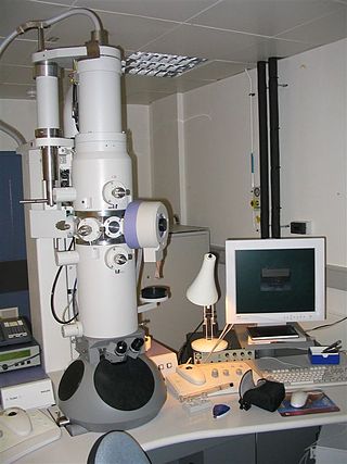
Transmission electron microscopy (TEM) is a microscopy technique in which a beam of electrons is transmitted through a specimen to form an image. The specimen is most often an ultrathin section less than 100 nm thick or a suspension on a grid. An image is formed from the interaction of the electrons with the sample as the beam is transmitted through the specimen. The image is then magnified and focused onto an imaging device, such as a fluorescent screen, a layer of photographic film, or a detector such as a scintillator attached to a charge-coupled device or a direct electron detector.
Scanning probe microscopy (SPM) is a branch of microscopy that forms images of surfaces using a physical probe that scans the specimen. SPM was founded in 1981, with the invention of the scanning tunneling microscope, an instrument for imaging surfaces at the atomic level. The first successful scanning tunneling microscope experiment was done by Gerd Binnig and Heinrich Rohrer. The key to their success was using a feedback loop to regulate gap distance between the sample and the probe.

An X-ray microscope uses electromagnetic radiation in the X-ray band to produce magnified images of objects. Since X-rays penetrate most objects, there is no need to specially prepare them for X-ray microscopy observations.
Electron backscatter diffraction (EBSD) is a scanning electron microscopy (SEM) technique used to study the crystallographic structure of materials. EBSD is carried out in a scanning electron microscope equipped with an EBSD detector comprising at least a phosphorescent screen, a compact lens and a low-light camera. In the microscope an incident beam of electrons hits a tilted sample. As backscattered electrons leave the sample, they interact with the atoms and are both elastically diffracted and lose energy, leaving the sample at various scattering angles before reaching the phosphor screen forming Kikuchi patterns (EBSPs). The EBSD spatial resolution depends on many factors, including the nature of the material under study and the sample preparation. They can be indexed to provide information about the material's grain structure, grain orientation, and phase at the micro-scale. EBSD is used for impurities and defect studies, plastic deformation, and statistical analysis for average misorientation, grain size, and crystallographic texture. EBSD can also be combined with energy-dispersive X-ray spectroscopy (EDS), cathodoluminescence (CL), and wavelength-dispersive X-ray spectroscopy (WDS) for advanced phase identification and materials discovery.
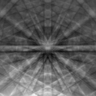
Electron crystallography is a subset of methods in electron diffraction focusing upon detailed determination of the positions of atoms in solids using a transmission electron microscope (TEM). It can involve the use of high-resolution transmission electron microscopy images, electron diffraction patterns including convergent-beam electron diffraction or combinations of these. It has been successful in determining some bulk structures, and also surface structures. Two related methods are low-energy electron diffraction which has solved the structure of many surfaces, and reflection high-energy electron diffraction which is used to monitor surfaces often during growth.

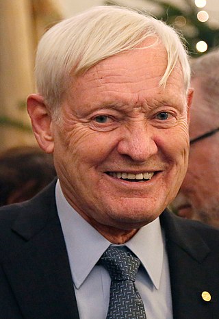
Richard Henderson is a British molecular biologist and biophysicist and pioneer in the field of electron microscopy of biological molecules. Henderson shared the Nobel Prize in Chemistry in 2017 with Jacques Dubochet and Joachim Frank. "Thanks to his work, we can look at individual atoms of living nature, thanks to cryo-electron microscopes we can see details without destroying samples, and for this he won the Nobel Prize in Chemistry."

JEOL, Ltd. is a major developer and manufacturer of electron microscopes and other scientific instruments, industrial equipment and medical equipment.
The Microscopy Society of America (MSA) was founded in 1942 as The Electron Microscope Society of America and is a non-profit organization that provides microanalytical facilities for studies within the sciences. Currently, there are approximately 3000 members. The society holds an annual meeting, which is usually held in the beginning of August. It has 30 local affiliates across the United States. The society has a program for examining and certifying technologists of electron microscopes. The organization produces two journals: Microscopy Today, and Microscopy and Microanalysis. As of 2024, the President is Jay Potts.

Microscopy and Microanalysis is a peer-reviewed scientific journal that covers original research in the fields of microscopy, imaging, and compositional analysis, including electron microscopy, fluorescence microscopy, atomic force microscopy, and live-cell imaging. It is published for the Microscopy Society of America.

Microscopy Research and Technique is a peer-reviewed scientific journal covering all areas of advanced microscopy in the biological, clinical, chemical, and materials science fields. The journal's title changed from Journal of Electron Microscopy Technique in 1992.
Food Structure was a peer-reviewed scientific journal which specialized in electron microscopy of foods, feeds, and their ingredients in addition to other methods of structural research including all kinds of optical microscopy. It was printed on glossy paper to ensure high quality of micrographs. It is not published any more but all papers are available at no charge and without registration.

ACS Photonics is a monthly, peer-reviewed, scientific journal, first published in January 2014 by the American Chemical Society. The current editor in chief is Romain Quidant. The interdisciplinary journal publishes original research articles, letters, comments, reviews and perspectives.

Paul Anthony Midgley FRS is a Professor of Materials Science in the Department of Materials Science and Metallurgy at the University of Cambridge and a fellow of Peterhouse, Cambridge.

John Charles Howorth Spence ForMemRS HonFRMS was Richard Snell Professor of Physics at Arizona State University and Director of Science at the National Science Foundation BioXFEL Science and Technology Center.
Joachim Frank ; born September 12, 1940) is a German-American biophysicist at Columbia University and a Nobel laureate. He is regarded as the founder of single-particle cryo-electron microscopy (cryo-EM), for which he shared the Nobel Prize in Chemistry in 2017 with Jacques Dubochet and Richard Henderson. He also made significant contributions to structure and function of the ribosome from bacteria and eukaryotes.

Cryogenic electron microscopy (cryo-EM) is a cryomicroscopy technique applied on samples cooled to cryogenic temperatures. For biological specimens, the structure is preserved by embedding in an environment of vitreous ice. An aqueous sample solution is applied to a grid-mesh and plunge-frozen in liquid ethane or a mixture of liquid ethane and propane. While development of the technique began in the 1970s, recent advances in detector technology and software algorithms have allowed for the determination of biomolecular structures at near-atomic resolution. This has attracted wide attention to the approach as an alternative to X-ray crystallography or NMR spectroscopy for macromolecular structure determination without the need for crystallization.
John Marius Rodenburg is emeritus professor in the Department of Electronic and Electrical Engineering at the University of Sheffield. He was elected a Fellow of the Royal Society (FRS) in 2019 for "internationally recognised... work on revolutionising the imaging capability of light, X-ray and electron transmission microscopes".
