
An integrated circuit is a set of electronic circuits on one small flat piece of semiconductor material, usually silicon. Large numbers of miniaturized transistors and other electronic components are integrated together on the chip. This results in circuits that are orders of magnitude smaller, faster, and less expensive than those constructed of discrete components, allowing a large transistor count.

Semiconductor device fabrication is the process used to manufacture semiconductor devices, typically integrated circuits (ICs) such as computer processors, microcontrollers, and memory chips that are present in everyday electrical and electronic devices. It is a multiple-step photolithographic and physio-chemical process during which electronic circuits are gradually created on a wafer, typically made of pure single-crystal semiconducting material. Silicon is almost always used, but various compound semiconductors are used for specialized applications.
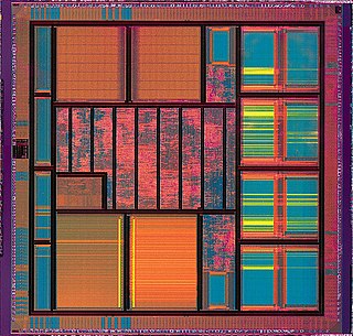
Very large-scale integration (VLSI) is the process of creating an integrated circuit (IC) by combining millions or billions of MOS transistors onto a single chip. VLSI began in the 1970s when MOS integrated circuit chips were developed and then widely adopted, enabling complex semiconductor and telecommunication technologies. The microprocessor and memory chips are VLSI devices.

An application-specific integrated circuit is an integrated circuit (IC) chip customized for a particular use, rather than intended for general-purpose use, such as a chip designed to run in a digital voice recorder or a high-efficiency video codec. Application-specific standard product chips are intermediate between ASICs and industry standard integrated circuits like the 7400 series or the 4000 series. ASIC chips are typically fabricated using metal–oxide–semiconductor (MOS) technology, as MOS integrated circuit chips.

Flip chip, also known as controlled collapse chip connection or its abbreviation, C4, is a method for interconnecting dies such as semiconductor devices, IC chips, integrated passive devices and microelectromechanical systems (MEMS), to external circuitry with solder bumps that have been deposited onto the chip pads. The technique was developed by General Electric's Light Military Electronics Department, Utica, New York. The solder bumps are deposited on the chip pads on the top side of the wafer during the final wafer processing step. In order to mount the chip to external circuitry, it is flipped over so that its top side faces down, and aligned so that its pads align with matching pads on the external circuit, and then the solder is reflowed to complete the interconnect. This is in contrast to wire bonding, in which the chip is mounted upright and fine wires are welded onto the chip pads and lead frame contacts to interconnect the chip pads to external circuitry.
Wafer fabrication is a procedure composed of many repeated sequential processes to produce complete electrical or photonic circuits on semiconductor wafers in semiconductor device fabrication process. Examples include production of radio frequency (RF) amplifiers, LEDs, optical computer components, and microprocessors for computers. Wafer fabrication is used to build components with the necessary electrical structures.
In semiconductor fabrication, a resist is a thin layer used to transfer a circuit pattern to the semiconductor substrate which it is deposited upon. A resist can be patterned via lithography to form a (sub)micrometer-scale, temporary mask that protects selected areas of the underlying substrate during subsequent processing steps. The material used to prepare said thin layer is typically a viscous solution. Resists are generally proprietary mixtures of a polymer or its precursor and other small molecules that have been specially formulated for a given lithography technology. Resists used during photolithography are called photoresists.
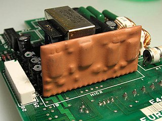
A hybrid integrated circuit (HIC), hybrid microcircuit, hybrid circuit or simply hybrid is a miniaturized electronic circuit constructed of individual devices, such as semiconductor devices and passive components, bonded to a substrate or printed circuit board (PCB). A PCB having components on a Printed Wiring Board (PWB) is not considered a true hybrid circuit according to the definition of MIL-PRF-38534.

The back end of line (BEOL) is the second portion of IC fabrication where the individual devices get interconnected with wiring on the wafer, the metalization layer. Common metals are copper and aluminum. BEOL generally begins when the first layer of metal is deposited on the wafer. BEOL includes contacts, insulating layers (dielectrics), metal levels, and bonding sites for chip-to-package connections.

A multi-chip module (MCM) is generically an electronic assembly where multiple integrated circuits, semiconductor dies and/or other discrete components are integrated, usually onto a unifying substrate, so that in use it can be treated as if it were a larger IC. Other terms for MCM packaging include "heterogeneous integration" or "hybrid integrated circuit". The advantage of using MCM packaging is it allows a manufacturer to use multiple components for modularity and/or to improve yields over a conventional monolithic IC approach.

Integrated circuit design, or IC design, is a sub-field of electronics engineering, encompassing the particular logic and circuit design techniques required to design integrated circuits, or ICs. ICs consist of miniaturized electronic components built into an electrical network on a monolithic semiconductor substrate by photolithography.

A system in a package (SiP) or system-in-package is a number of integrated circuits (ICs) enclosed in one chip carrier package or encompassing an IC package substrate that may include passive components and perform the functions of an entire system. The ICs may be stacked using package on package, placed side by side, and/or embedded in the substrate. The SiP performs all or most of the functions of an electronic system, and is typically used when designing components for mobile phones, digital music players, etc. Dies containing integrated circuits may be stacked vertically on a substrate. They are internally connected by fine wires that are bonded to the package. Alternatively, with a flip chip technology, solder bumps are used to join stacked chips together. SiPs are like systems on a chip (SoCs) but less tightly integrated and not on a single semiconductor die.
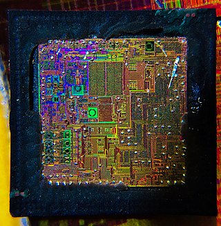
A die, in the context of integrated circuits, is a small block of semiconducting material on which a given functional circuit is fabricated. Typically, integrated circuits are produced in large batches on a single wafer of electronic-grade silicon (EGS) or other semiconductor through processes such as photolithography. The wafer is cut (diced) into many pieces, each containing one copy of the circuit. Each of these pieces is called a die.

Multi-project chip (MPC), and multi-project wafer (MPW) semiconductor manufacturing arrangements allow customers to share mask and microelectronics wafer fabrication cost between several designs or projects.

In electronic engineering, a through-silicon via (TSV) or through-chip via is a vertical electrical connection (via) that passes completely through a silicon wafer or die. TSVs are high-performance interconnect techniques used as an alternative to wire-bond and flip chips to create 3D packages and 3D integrated circuits. Compared to alternatives such as package-on-package, the interconnect and device density is substantially higher, and the length of the connections becomes shorter.
A three-dimensional integrated circuit is a MOS integrated circuit (IC) manufactured by stacking as many as 16 or more ICs and interconnecting them vertically using, for instance, through-silicon vias (TSVs) or Cu-Cu connections, so that they behave as a single device to achieve performance improvements at reduced power and smaller footprint than conventional two dimensional processes. The 3D IC is one of several 3D integration schemes that exploit the z-direction to achieve electrical performance benefits in microelectronics and nanoelectronics.

Integrated passive devices (IPDs), also known as integrated passive components (IPCs) or embedded passive components (EPC), are electronic components where resistors (R), capacitors (C), inductors (L)/coils/chokes, microstriplines, impedance matching elements, baluns or any combinations of them are integrated in the same package or on the same substrate. Sometimes integrated passives can also be called as embedded passives, and still the difference between integrated and embedded passives is technically unclear. In both cases passives are realized in between dielectric layers or on the same substrate.

Wafer-level packaging (WLP) is a process where packaging components are attached to an integrated circuit (IC) before the wafer – on which the IC is fabricated – is diced. In WSP, the top and bottom layers of the packaging and the solder bumps are attached to the integrated circuits while they are still in the wafer. This process differs from a conventional process, in which the wafer is sliced into individual circuits (dice) before the packaging components are attached.
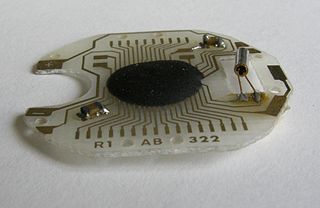
Chip on board (COB) is a method of circuit board manufacturing in which the integrated circuits (e.g. microprocessors) are attached (wired, bonded directly) to a printed circuit board, and covered by a blob of epoxy. By eliminating the packaging of individual semiconductor devices, the completed product can be more compact, lighter, and less costly. In some cases, COB construction improves the operation of radio frequency systems by reducing the inductance and capacitance of integrated circuit leads.
Advanced packaging is the aggregation and interconnection of components before traditional integrated circuit packaging. Advanced packaging allows multiple devices to be merged and packaged as a single electronic device. Unlike traditional integrated circuit packaging, advanced packaging employs processes and techniques that are performed at semiconductor fabrication facilities. Advanced packaging thus sits between fabrication and traditional packaging -- or, in other terminology, between BEoL and post-fab. Advanced packaging includes multi-chip modules, 3D ICs, 2.5D ICs, heterogeneous integration, fan-out wafer-level packaging, system-in-package, quilt packaging, combining logic (processors) and memory in a single package, die stacking, several chiplets or dies in a package, combinations of these techniques, and others.