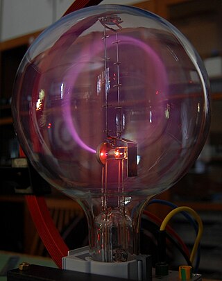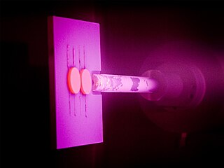
Cathode rays or electron beams (e-beam) are streams of electrons observed in discharge tubes. If an evacuated glass tube is equipped with two electrodes and a voltage is applied, glass behind the positive electrode is observed to glow, due to electrons emitted from the cathode. They were first observed in 1859 by German physicist Julius Plücker and Johann Wilhelm Hittorf, and were named in 1876 by Eugen Goldstein Kathodenstrahlen, or cathode rays. In 1897, British physicist J. J. Thomson showed that cathode rays were composed of a previously unknown negatively charged particle, which was later named the electron. Cathode-ray tubes (CRTs) use a focused beam of electrons deflected by electric or magnetic fields to render an image on a screen.

In physics, sputtering is a phenomenon in which microscopic particles of a solid material are ejected from its surface, after the material is itself bombarded by energetic particles of a plasma or gas. It occurs naturally in outer space, and can be an unwelcome source of wear in precision components. However, the fact that it can be made to act on extremely fine layers of material is utilised in science and industry—there, it is used to perform precise etching, carry out analytical techniques, and deposit thin film layers in the manufacture of optical coatings, semiconductor devices and nanotechnology products. It is a physical vapor deposition technique.

Electroplating, also known as electrochemical deposition or electrodeposition, is a process for producing a metal coating on a solid substrate through the reduction of cations of that metal by means of a direct electric current. The part to be coated acts as the cathode of an electrolytic cell; the electrolyte is a solution of a salt of the metal to be coated; and the anode is usually either a block of that metal, or of some inert conductive material. The current is provided by an external power supply.

An ion source is a device that creates atomic and molecular ions. Ion sources are used to form ions for mass spectrometers, optical emission spectrometers, particle accelerators, ion implanters and ion engines.
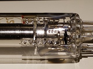
An electron gun is an electrical component in some vacuum tubes that produces a narrow, collimated electron beam that has a precise kinetic energy.

Pulsed laser deposition (PLD) is a physical vapor deposition (PVD) technique where a high-power pulsed laser beam is focused inside a vacuum chamber to strike a target of the material that is to be deposited. This material is vaporized from the target which deposits it as a thin film on a substrate. This process can occur in ultra high vacuum or in the presence of a background gas, such as oxygen which is commonly used when depositing oxides to fully oxygenate the deposited films.

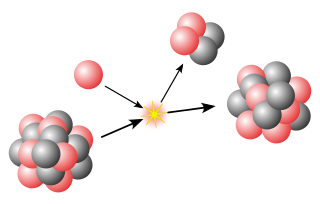
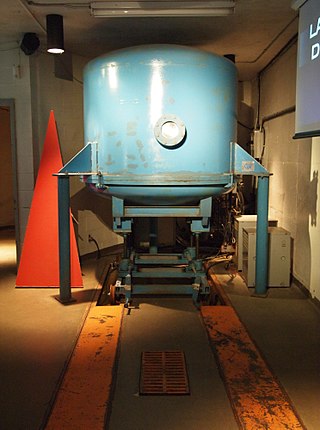
Neutron generators are neutron source devices which contain compact linear particle accelerators and that produce neutrons by fusing isotopes of hydrogen together. The fusion reactions take place in these devices by accelerating either deuterium, tritium, or a mixture of these two isotopes into a metal hydride target which also contains deuterium, tritium or a mixture of these isotopes. Fusion of deuterium atoms results in the formation of a helium-3 ion and a neutron with a kinetic energy of approximately 2.5 MeV. Fusion of a deuterium and a tritium atom results in the formation of a helium-4 ion and a neutron with a kinetic energy of approximately 14.1 MeV. Neutron generators have applications in medicine, security, and materials analysis.

A glow discharge is a plasma formed by the passage of electric current through a gas. It is often created by applying a voltage between two electrodes in a glass tube containing a low-pressure gas. When the voltage exceeds a value called the striking voltage, the gas ionization becomes self-sustaining, and the tube glows with a colored light. The color depends on the gas used.
A thin film is a layer of material ranging from fractions of a nanometer (monolayer) to several micrometers in thickness. The controlled synthesis of materials as thin films is a fundamental step in many applications. A familiar example is the household mirror, which typically has a thin metal coating on the back of a sheet of glass to form a reflective interface. The process of silvering was once commonly used to produce mirrors, while more recently the metal layer is deposited using techniques such as sputtering. Advances in thin film deposition techniques during the 20th century have enabled a wide range of technological breakthroughs in areas such as magnetic recording media, electronic semiconductor devices, integrated passive devices, LEDs, optical coatings, hard coatings on cutting tools, and for both energy generation and storage. It is also being applied to pharmaceuticals, via thin-film drug delivery. A stack of thin films is called a multilayer.
A vacuum arc can arise when the surfaces of metal electrodes in contact with a good vacuum begin to emit electrons either through heating or in an electric field that is sufficient to cause field electron emission. Once initiated, a vacuum arc can persist, since the freed particles gain kinetic energy from the electric field, heating the metal surfaces through high-speed particle collisions. This process can create an incandescent cathode spot, which frees more particles, thereby sustaining the arc. At sufficiently high currents an incandescent anode spot may also be formed.

Electrophoretic deposition (EPD), is a term for a broad range of industrial processes which includes electrocoating, cathodic electrodeposition, anodic electrodeposition, and electrophoretic coating, or electrophoretic painting. A characteristic feature of this process is that colloidal particles suspended in a liquid medium migrate under the influence of an electric field (electrophoresis) and are deposited onto an electrode. All colloidal particles that can be used to form stable suspensions and that can carry a charge can be used in electrophoretic deposition. This includes materials such as polymers, pigments, dyes, ceramics and metals.
Electron-beam physical vapor deposition, or EBPVD, is a form of physical vapor deposition in which a target anode is bombarded with an electron beam given off by a charged tungsten filament under high vacuum. The electron beam causes atoms from the target to transform into the gaseous phase. These atoms then precipitate into solid form, coating everything in the vacuum chamber with a thin layer of the anode material.

Vacuum deposition is a group of processes used to deposit layers of material atom-by-atom or molecule-by-molecule on a solid surface. These processes operate at pressures well below atmospheric pressure. The deposited layers can range from a thickness of one atom up to millimeters, forming freestanding structures. Multiple layers of different materials can be used, for example to form optical coatings. The process can be qualified based on the vapor source; physical vapor deposition uses a liquid or solid source and chemical vapor deposition uses a chemical vapor.

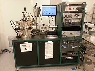
Physical vapor deposition (PVD), sometimes called physical vapor transport (PVT), describes a variety of vacuum deposition methods which can be used to produce thin films and coatings on substrates including metals, ceramics, glass, and polymers. PVD is characterized by a process in which the material transitions from a condensed phase to a vapor phase and then back to a thin film condensed phase. The most common PVD processes are sputtering and evaporation. PVD is used in the manufacturing of items which require thin films for optical, mechanical, electrical, acoustic or chemical functions. Examples include semiconductor devices such as thin-film solar cells, microelectromechanical devices such as thin film bulk acoustic resonator, aluminized PET film for food packaging and balloons, and titanium nitride coated cutting tools for metalworking. Besides PVD tools for fabrication, special smaller tools used mainly for scientific purposes have been developed.

Thermal spraying techniques are coating processes in which melted materials are sprayed onto a surface. The "feedstock" is heated by electrical or chemical means.
Plasma activation is a method of surface modification employing plasma processing, which improves surface adhesion properties of many materials including metals, glass, ceramics, a broad range of polymers and textiles and even natural materials such as wood and seeds. Plasma functionalization also refers to the introduction of functional groups on the surface of exposed materials. It is widely used in industrial processes to prepare surfaces for bonding, gluing, coating and painting. Plasma processing achieves this effect through a combination of reduction of metal oxides, ultra-fine surface cleaning from organic contaminants, modification of the surface topography and deposition of functional chemical groups. Importantly, the plasma activation can be performed at atmospheric pressure using air or typical industrial gases including hydrogen, nitrogen and oxygen. Thus, the surface functionalization is achieved without expensive vacuum equipment or wet chemistry, which positively affects its costs, safety and environmental impact. Fast processing speeds further facilitate numerous industrial applications.

Evaporation is a common method of thin-film deposition. The source material is evaporated in a vacuum. The vacuum allows vapor particles to travel directly to the target object (substrate), where they condense back to a solid state. Evaporation is used in microfabrication, and to make macro-scale products such as metallized plastic film.

Sputter deposition is a physical vapor deposition (PVD) method of thin film deposition by the phenomenon of sputtering. This involves ejecting material from a "target" that is a source onto a "substrate" such as a silicon wafer. Resputtering is re-emission of the deposited material during the deposition process by ion or atom bombardment. Sputtered atoms ejected from the target have a wide energy distribution, typically up to tens of eV. The sputtered ions can ballistically fly from the target in straight lines and impact energetically on the substrates or vacuum chamber. Alternatively, at higher gas pressures, the ions collide with the gas atoms that act as a moderator and move diffusively, reaching the substrates or vacuum chamber wall and condensing after undergoing a random walk. The entire range from high-energy ballistic impact to low-energy thermalized motion is accessible by changing the background gas pressure. The sputtering gas is often an inert gas such as argon. For efficient momentum transfer, the atomic weight of the sputtering gas should be close to the atomic weight of the target, so for sputtering light elements neon is preferable, while for heavy elements krypton or xenon are used. Reactive gases can also be used to sputter compounds. The compound can be formed on the target surface, in-flight or on the substrate depending on the process parameters. The availability of many parameters that control sputter deposition make it a complex process, but also allow experts a large degree of control over the growth and microstructure of the film.
High-power impulse magnetron sputtering is a method for physical vapor deposition of thin films which is based on magnetron sputter deposition. HIPIMS utilises extremely high power densities of the order of kW⋅cm−2 in short pulses (impulses) of tens of microseconds at low duty cycle of < 10%. Distinguishing features of HIPIMS are a high degree of ionisation of the sputtered metal and a high rate of molecular gas dissociation which result in high density of deposited films. The ionization and dissociation degree increase according to the peak cathode power. The limit is determined by the transition of the discharge from glow to arc phase. The peak power and the duty cycle are selected so as to maintain an average cathode power similar to conventional sputtering (1–10 W⋅cm−2).

Titanium aluminium nitride (TiAlN) or aluminium titanium nitride is a group of metastable hard coatings consisting of nitrogen and the metallic elements aluminium and titanium. This compound as well as similar compounds(such as TiN and TiCN) are most notably used for coating machine tools such and endmills and drills to change their properties, such as increased thermal stability and/or wear resistance. Four important compositions are deposited in industrial scale by physical vapor deposition methods:


