Related Research Articles

A printed circuit board (PCB), also called printed wiring board (PWB), is a laminated sandwich structure of conductive and insulating layers, each with a pattern of traces, planes and other features etched from one or more sheet layers of copper laminated onto or between sheet layers of a non-conductive substrate. PCBs are used to connect or "wire" components to one another in an electronic circuit. Electrical components may be fixed to conductive pads on the outer layers, generally by soldering, which both electrically connects and mechanically fastens the components to the board. Another manufacturing process adds vias, metal-lined drilled holes that enable electrical interconnections between conductive layers, to boards with more than a single side.
A microtome is a cutting tool used to produce extremely thin slices of material known as sections, with the process being termed microsectioning. Important in science, microtomes are used in microscopy for the preparation of samples for observation under transmitted light or electron radiation.
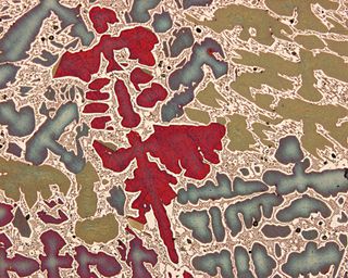
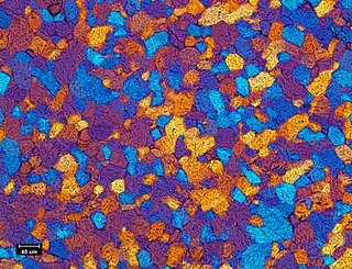
Metallography is the study of the physical structure and components of metals, by using microscopy.

Focused ion beam, also known as FIB, is a technique used particularly in the semiconductor industry, materials science and increasingly in the biological field for site-specific analysis, deposition, and ablation of materials. A FIB setup is a scientific instrument that resembles a scanning electron microscope (SEM). However, while the SEM uses a focused beam of electrons to image the sample in the chamber, a FIB setup uses a focused beam of ions instead. FIB can also be incorporated in a system with both electron and ion beam columns, allowing the same feature to be investigated using either of the beams. FIB should not be confused with using a beam of focused ions for direct write lithography. These are generally quite different systems where the material is modified by other mechanisms.
This article is a list of terms commonly used in the practice of metalworking – the science, art, industry, and craft of shaping metal.

Flat no-leads packages such as quad-flat no-leads (QFN) and dual-flat no-leads (DFN) physically and electrically connect integrated circuits to printed circuit boards. Flat no-leads, also known as micro leadframe (MLF) and SON, is a surface-mount technology, one of several package technologies that connect ICs to the surfaces of PCBs without through-holes. Flat no-lead is a near chip scale plastic encapsulated package made with a planar copper lead frame substrate. Perimeter lands on the package bottom provide electrical connections to the PCB. Flat no-lead packages usually, but not always, include an exposed thermally conductive pad to improve heat transfer out of the IC. Heat transfer can be further facilitated by metal vias in the thermal pad. The QFN package is similar to the quad-flat package (QFP), and a ball grid array (BGA).
Ceramography is the art and science of preparation, examination and evaluation of ceramic microstructures. Ceramography can be thought of as the metallography of ceramics. The microstructure is the structure level of approximately 0.1 to 100 μm, between the minimum wavelength of visible light and the resolution limit of the naked eye. The microstructure includes most grains, secondary phases, grain boundaries, pores, micro-cracks and hardness microindentations. Most bulk mechanical, optical, thermal, electrical and magnetic properties are significantly affected by the microstructure. The fabrication method and process conditions are generally indicated by the microstructure. The root cause of many ceramic failures is evident in the microstructure. Ceramography is part of the broader field of materialography, which includes all the microscopic techniques of material analysis, such as metallography, petrography and plastography. Ceramography is usually reserved for high-performance ceramics for industrial applications, such as 85–99.9% alumina (Al2O3) in Fig. 1, zirconia (ZrO2), silicon carbide (SiC), silicon nitride (Si3N4), and ceramic-matrix composites. It is seldom used on whiteware ceramics such as sanitaryware, wall tiles and dishware.
Acoustic microscopy is microscopy that employs very high or ultra high frequency ultrasound. Acoustic microscopes operate non-destructively and penetrate most solid materials to make visible images of internal features, including defects such as cracks, delaminations and voids.

Thick-film technology is used to produce electronic devices/modules such as surface mount devices modules, hybrid integrated circuits, heating elements, integrated passive devices and sensors. The main manufacturing technique is screen printing (stenciling), which in addition to use in manufacturing electronic devices can also be used for various graphic reproduction targets. It became one of the key manufacturing/miniaturisation techniques of electronic devices/modules during 1950s. Typical film thickness – manufactured with thick film manufacturing processes for electronic devices – is 0.0001 to 0.1 mm.
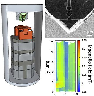
In condensed matter physics, scanning SQUID microscopy is a technique where a superconducting quantum interference device (SQUID) is used to image surface magnetic field strength with micrometre-scale resolution. A tiny SQUID is mounted onto a tip which is then rastered near the surface of the sample to be measured. As the SQUID is the most sensitive detector of magnetic fields available and can be constructed at submicrometre widths via lithography, the scanning SQUID microscope allows magnetic fields to be measured with unparalleled resolution and sensitivity. The first scanning SQUID microscope was built in 1992 by Black et al. Since then the technique has been used to confirm unconventional superconductivity in several high-temperature superconductors including YBCO and BSCCO compounds.
Electronic components have a wide range of failure modes. These can be classified in various ways, such as by time or cause. Failures can be caused by excess temperature, excess current or voltage, ionizing radiation, mechanical shock, stress or impact, and many other causes. In semiconductor devices, problems in the device package may cause failures due to contamination, mechanical stress of the device, or open or short circuits.
Diamond grinding is a pavement preservation technique that corrects a variety of surface imperfections on both concrete and asphalt concrete pavements. Most often utilized on concrete pavement, diamond grinding is typically performed in conjunction with other concrete pavement preservation (CPP) techniques such as road slab stabilization, full- and partial-depth repair, dowel bar retrofit, cross stitching longitudinal cracks or joints and joint and crack resealing. Diamond grinding restores rideability by removing surface irregularities caused during construction or through repeated traffic loading over time. The immediate effect of diamond grinding is a significant improvement in the smoothness of a pavement. Another important effect of diamond grinding is the considerable increase in surface macrotexture and consequent improvement in skid resistance, noise reduction and safety.
Ion milling is a specialized physical etching technique that is a crucial step in the preparation of material analysis techniques. After a specimen goes through ion milling, the surface becomes much smoother and more defined, which allows scientists to study the material much easier. The ion mill generates high-energy particles to remove material off the surface of a specimen, similar to how sand and dust particles wear away at rocks in a canyon to create a smooth surface. Relative to other techniques, ion milling creates much less surface damage, which makes it perfect for surface-sensitive analytical techniques. This article discusses the principle, equipment, applications, and significance of ion milling.
Pad cratering is a mechanically induced fracture in the resin between copper foil and outermost layer of fiberglass of a printed circuit board (PCB). It may be within the resin or at the resin to fiberglass interface.
Glass frit bonding, also referred to as glass soldering or seal glass bonding, describes a wafer bonding technique with an intermediate glass layer. It is a widely used encapsulation technology for surface micro-machined structures, e.g., accelerometers or gyroscopes. The technique utilizes low melting-point glass and therefore provides various advantages including that viscosity of glass decreases with an increase of temperature. The viscous flow of glass has effects to compensate and planarize surface irregularities, convenient for bonding wafers with a high roughness due to plasma etching or deposition. A low viscosity promotes hermetically sealed encapsulation of structures based on a better adaption of the structured shapes. Further, the coefficient of thermal expansion (CTE) of the glass material is adapted to silicon. This results in low stress in the bonded wafer pair. The glass has to flow and wet the soldered surfaces well below the temperature where deformation or degradation of either of the joined materials or nearby structures occurs. The usual temperature of achieving flowing and wetting is between 450 and 550 °C.
Stencil printing is the process of depositing solder paste on the printed wiring boards (PWBs) to establish electrical connections. It is immediately followed by the component placement stage. The equipment and materials used in this stage are a stencil, solder paste, and a printer.
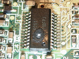
Decapping (decapsulation) or delidding of an integrated circuit (IC) is the process of removing the protective cover or integrated heat spreader (IHS) of an integrated circuit so that the contained die is revealed for visual inspection of the micro circuitry imprinted on the die. This process is typically done in order to debug a manufacturing problem with the chip, or possibly to copy information from the device, to check for counterfeit chips or to reverse engineer it. Companies such as TechInsights and ChipRebel decap, take die shots of, and reverse engineer chips for customers. Modern integrated circuits can be encapsulated in plastic, ceramic, or epoxy packages.
Digital image correlation analyses have applications in material property characterization, displacement measurement, and strain mapping. As such, DIC is becoming an increasingly popular tool when evaluating the thermo-mechanical behavior of electronic components and systems.
Dye-n-Pry, also called Dye And Pry, Dye and Pull, Dye Staining, or Dye Penetrant, is a destructive analysis technique used on surface mount technology (SMT) components to either perform failure analysis or inspect for solder joint integrity. It is an application of dye penetrant inspection.

Printed circuit board manufacturing is the process of manufacturing bare printed circuit boards (PCBs) and populating them with electronic components. It includes all the processes to produce the full assembly of a board into a functional circuit board.
References
- ↑ Robertson, Christopher T (2004). Printed Circuit Board Designer's Reference: Basics. Prentice Hall Professional. p. 45. ISBN 9780130674814.
- ↑ "Circuits Assembly Online Magazine - Using Cross-Sectioning for PCB Assembly Qualification".
- 1 2 "From transistors to bumps: Preparing SEM cross-sections by combining site-specific cleaving and broad ion milling" (PDF). Solid State Technology. Archived from the original on 2017-11-14. Retrieved 2024-12-04.
- ↑ "PCB Microsectioning – Circuit Board Cross Section | saturn". Archived from the original on 2017-12-01. Retrieved 2017-10-30.
- ↑ "Allied High Tech Products - Mechanical Milling".
- ↑ "Abrasive Cutting Techniques: Cutting Mode". buehler.com.
- ↑ "Precision Cutting - The Science of the Cut" (PDF). buehler.com.
- ↑ https://www.circuitinsight.com/pdf/alternative_methods_cross_sectioning_smta.pdf [ bare URL PDF ]
- ↑ Dusek, Milos; Hunt, Christopher (March 2004). "Crack Detection Methods For Lead-free Solder Joints" (PDF). National Physical Laboratory. ISSN 1473-2734. Archived (PDF) from the original on 2017-08-29. Retrieved 2017-10-13.
- ↑ https://nepp.nasa.gov/docuploads/D084F3EB-BFA9-4733-8F535584A99095F9/Dernning_BGAInspection.pdf [ bare URL PDF ]