
Computer memory stores information, such as data and programs, for immediate use in the computer. The term memory is often synonymous with the terms RAM,main memory or primary storage. Archaic synonyms for main memory include core and store.

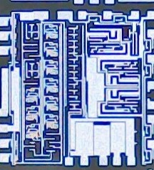
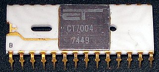
An integrated circuit (IC), also known as a microchip, computer chip, or simply chip, is a small electronic device made up of multiple interconnected electronic components such as transistors, resistors, and capacitors. These components are etched onto a small piece of semiconductor material, usually silicon. Integrated circuits are used in a wide range of electronic devices, including computers, smartphones, and televisions, to perform various functions such as processing and storing information. They have greatly impacted the field of electronics by enabling device miniaturization and enhanced functionality.

The StrongARM is a family of computer microprocessors developed by Digital Equipment Corporation and manufactured in the late 1990s which implemented the ARM v4 instruction set architecture. It was later acquired by Intel in 1997 from DEC's own Digital Semiconductor division as part of a settlement of a lawsuit between the two companies over patent infringement. Intel then continued to manufacture it before replacing it with the StrongARM-derived ARM-based follow-up architecture called XScale in the early 2000s.

Complementary metal–oxide–semiconductor is a type of metal–oxide–semiconductor field-effect transistor (MOSFET) fabrication process that uses complementary and symmetrical pairs of p-type and n-type MOSFETs for logic functions. CMOS technology is used for constructing integrated circuit (IC) chips, including microprocessors, microcontrollers, memory chips, and other digital logic circuits. CMOS technology is also used for analog circuits such as image sensors, data converters, RF circuits, and highly integrated transceivers for many types of communication.

In electronics and especially synchronous digital circuits, a clock signal is an electronic logic signal which oscillates between a high and a low state at a constant frequency and is used like a metronome to synchronize actions of digital circuits. In a synchronous logic circuit, the most common type of digital circuit, the clock signal is applied to all storage devices, flip-flops and latches, and causes them all to change state simultaneously, preventing race conditions.
In computer engineering, a logic family is one of two related concepts:
A mixed-signal integrated circuit is any integrated circuit that has both analog circuits and digital circuits on a single semiconductor die. Their usage has grown dramatically with the increased use of cell phones, telecommunications, portable electronics, and automobiles with electronics and digital sensors.
Semiconductor memory is a digital electronic semiconductor device used for digital data storage, such as computer memory. It typically refers to devices in which data is stored within metal–oxide–semiconductor (MOS) memory cells on a silicon integrated circuit memory chip. There are numerous different types using different semiconductor technologies. The two main types of random-access memory (RAM) are static RAM (SRAM), which uses several transistors per memory cell, and dynamic RAM (DRAM), which uses a transistor and a MOS capacitor per cell. Non-volatile memory uses floating-gate memory cells, which consist of a single floating-gate transistor per cell.

In integrated circuits, depletion-load NMOS is a form of digital logic family that uses only a single power supply voltage, unlike earlier NMOS logic families that needed more than one different power supply voltage. Although manufacturing these integrated circuits required additional processing steps, improved switching speed and the elimination of the extra power supply made this logic family the preferred choice for many microprocessors and other logic elements.
The transistor count is the number of transistors in an electronic device. It is the most common measure of integrated circuit complexity. The rate at which MOS transistor counts have increased generally follows Moore's law, which observes that transistor count doubles approximately every two years. However, being directly proportional to the area of a chip, transistor count does not represent how advanced the corresponding manufacturing technology is: a better indication of this is transistor density.
A field-programmable analog array (FPAA) is an integrated circuit device containing computational analog blocks (CAB) and interconnects between these blocks offering field-programmability. Unlike their digital cousin, the FPGA, the devices tend to be more application driven than general purpose as they may be current mode or voltage mode devices. For voltage mode devices, each block usually contains an operational amplifier in combination with programmable configuration of passive components. The blocks can, for example, act as summers or integrators.
Four-phase logic is a type of, and design methodology for dynamic logic. It enabled non-specialist engineers to design quite complex ICs, using either PMOS or NMOS processes. It uses a kind of 4-phase clock signal.
PMOS or pMOS logic is a family of digital circuits based on p-channel, enhancement mode metal–oxide–semiconductor field-effect transistors (MOSFETs). In the late 1960s and early 1970s, PMOS logic was the dominant semiconductor technology for large-scale integrated circuits before being superseded by NMOS and CMOS devices.

Asad Ali Abidi is a Pakistani-American electrical engineer. He serves as a tenured professor at University of California, Los Angeles, and is the inaugural holder of the Abdus Salam Chair at the Lahore University of Management Sciences (LUMS). He is best known for pioneering RF CMOS technology during the late 1980s to early 1990s. As of 2008, the radio transceivers in all wireless networking devices and modern mobile phones are mass-produced as RF CMOS devices.
Random-access memory is a form of electronic computer memory that can be read and changed in any order, typically used to store working data and machine code. A random-access memory device allows data items to be read or written in almost the same amount of time irrespective of the physical location of data inside the memory, in contrast with other direct-access data storage media, where the time required to read and write data items varies significantly depending on their physical locations on the recording medium, due to mechanical limitations such as media rotation speeds and arm movement.
Donhee Ham is the John A. and Elizabeth S. Armstrong Professor of Engineering and Applied Sciences at Harvard University and Fellow of Samsung Electronics.

The memory cell is the fundamental building block of computer memory. The memory cell is an electronic circuit that stores one bit of binary information and it must be set to store a logic 1 and reset to store a logic 0. Its value is maintained/stored until it is changed by the set/reset process. The value in the memory cell can be accessed by reading it.
RF CMOS is a metal–oxide–semiconductor (MOS) integrated circuit (IC) technology that integrates radio-frequency (RF), analog and digital electronics on a mixed-signal CMOS RF circuit chip. It is widely used in modern wireless telecommunications, such as cellular networks, Bluetooth, Wi-Fi, GPS receivers, broadcasting, vehicular communication systems, and the radio transceivers in all modern mobile phones and wireless networking devices. RF CMOS technology was pioneered by Pakistani engineer Asad Ali Abidi at UCLA during the late 1980s to early 1990s, and helped bring about the wireless revolution with the introduction of digital signal processing in wireless communications. The development and design of RF CMOS devices was enabled by van der Ziel's FET RF noise model, which was published in the early 1960s and remained largely forgotten until the 1990s.


