Propagation delay

Last updated

Propagation delay is the time duration taken for a signal to reach its destination. It can relate to networking, electronics or physics.

Contents

Networking

In computer networks, propagation delay is the amount of time it takes for the head of the signal to travel from the sender to the receiver. It can be computed as the ratio between the link length and the propagation speed over the specific medium.

Propagation delay is equal to d / s where d is the distance and s is the wave propagation speed. In wireless communication, s=c, i.e. the speed of light. In copper wire, the speed s generally ranges from .59c to .77c. [1] [2] This delay is the major obstacle in the development of high-speed computers and is called the interconnect bottleneck in IC systems.

Electronics

Propagation delay timing diagram of a NOT gate Propagation delay timing diagram.svg
Propagation delay timing diagram of a NOT gate
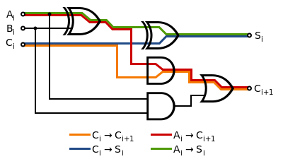
A full adder has an overall gate delay of 3 logic gates from the inputs A and B to the carry output Cout shown in red. Full-Adder Propagation Delay.svg
A full adder has an overall gate delay of 3 logic gates from the inputs A and B to the carry output Cout shown in red.

In electronics, digital circuits and digital electronics, the propagation delay, or gate delay, is the length of time which starts when the input to a logic gate becomes stable and valid to change, to the time that the output of that logic gate is stable and valid to change. Often on manufacturers' datasheets this refers to the time required for the output to reach 50% of its final output level from when the input changes to 50% of its final input level. This may depend on the direction of the level change, in which case separate fall and rise delays tPHL and tPLH or tf and tr are given. Reducing gate delays in digital circuits allows them to process data at a faster rate and improve overall performance. The determination of the propagation delay of a combined circuit requires identifying the longest path of propagation delays from input to output and by adding each propagation delay along this path.

The difference in propagation delays of logic elements is the major contributor to glitches in asynchronous circuits as a result of race conditions.

The principle of logical effort utilizes propagation delays to compare designs implementing the same logical statement.

Propagation delay increases with operating temperature, as resistance of conductive materials tends to increase with temperature. Marginal increases in supply voltage can increase propagation delay since the upper switching threshold voltage, VIH (often expressed as a percentage of the high-voltage supply rail), naturally increases proportionately. [3] Increases in output load capacitance, often from placing increased fan-out loads on a wire, will also increase propagation delay. All of these factors influence each other through an RC time constant: any increase in load capacitance increases C, heat-induced resistance the R factor, and supply threshold voltage increases will affect whether more than one time constants are required to reach the threshold. If the output of a logic gate is connected to a long trace or used to drive many other gates (high fanout) the propagation delay increases substantially.

Wires have an approximate propagation delay of 1 ns for every 6 inches (15 cm) of length. [4] Logic gates can have propagation delays ranging from more than 10 ns down to the picosecond range, depending on the technology being used. [4]

Physics

In physics, particularly in the electromagnetic field, the propagation delay is the length of time it takes for a signal to travel to its destination. For example, in the case of an electric signal, it is the time taken for the signal to travel through a wire. See also velocity factor and radio propagation.

See also

Related Research Articles

<span class="mw-page-title-main">Logic gate</span> Device performing a Boolean function

A logic gate is a device that performs a Boolean function, a logical operation performed on one or more binary inputs that produces a single binary output. Depending on the context, the term may refer to an ideal logic gate, one that has, for instance, zero rise time and unlimited fan-out, or it may refer to a non-ideal physical device.

Transistor–transistor logic (TTL) is a logic family built from bipolar junction transistors. Its name signifies that transistors perform both the logic function and the amplifying function, as opposed to earlier resistor–transistor logic (RTL) and diode–transistor logic (DTL).

<span class="mw-page-title-main">CMOS</span> Technology for constructing integrated circuits

Complementary metal–oxide–semiconductor is a type of metal–oxide–semiconductor field-effect transistor (MOSFET) fabrication process that uses complementary and symmetrical pairs of p-type and n-type MOSFETs for logic functions. CMOS technology is used for constructing integrated circuit (IC) chips, including microprocessors, microcontrollers, memory chips, and other digital logic circuits. CMOS technology is also used for analog circuits such as image sensors, data converters, RF circuits, and highly integrated transceivers for many types of communication.

<span class="mw-page-title-main">Emitter-coupled logic</span> Integrated circuit logic family

In electronics, emitter-coupled logic (ECL) is a high-speed integrated circuit bipolar transistor logic family. ECL uses an overdriven bipolar junction transistor (BJT) differential amplifier with single-ended input and limited emitter current to avoid the saturated region of operation and its slow turn-off behavior. As the current is steered between two legs of an emitter-coupled pair, ECL is sometimes called current-steering logic (CSL), current-mode logic (CML) or current-switch emitter-follower (CSEF) logic.

In digital electronics, the fan-out is the number of gate inputs driven by the output of another single logic gate.

Resistor–transistor logic (RTL), sometimes also known as transistor–resistor logic (TRL), is a class of digital circuits built using resistors as the input network and bipolar junction transistors (BJTs) as switching devices. RTL is the earliest class of transistorized digital logic circuit; it was succeeded by diode–transistor logic (DTL) and transistor–transistor logic (TTL).

<span class="mw-page-title-main">Diode–transistor logic</span>

Diode–transistor logic (DTL) is a class of digital circuits that is the direct ancestor of transistor–transistor logic. It is called so because the logic gating functions AND and OR are performed by diode logic, while logical inversion (NOT) and amplification is performed by a transistor.

In computer engineering, a logic family is one of two related concepts:

Asynchronous circuit is a sequential digital logic circuit that does not use a global clock circuit or signal generator to synchronize its components. Instead, the components are driven by a handshaking circuit which indicates a completion of a set of instructions. Handshaking works by simple data transfer protocols. Many synchronous circuits were developed in early 1950s as part of bigger asynchronous systems. Asynchronous circuits and theory surrounding is a part of several steps in integrated circuit design, a field of digital electronics engineering.

<span class="mw-page-title-main">Signal integrity</span>

Signal integrity or SI is a set of measures of the quality of an electrical signal. In digital electronics, a stream of binary values is represented by a voltage waveform. However, digital signals are fundamentally analog in nature, and all signals are subject to effects such as noise, distortion, and loss. Over short distances and at low bit rates, a simple conductor can transmit this with sufficient fidelity. At high bit rates and over longer distances or through various mediums, various effects can degrade the electrical signal to the point where errors occur and the system or device fails. Signal integrity engineering is the task of analyzing and mitigating these effects. It is an important activity at all levels of electronics packaging and assembly, from internal connections of an integrated circuit (IC), through the package, the printed circuit board (PCB), the backplane, and inter-system connections. While there are some common themes at these various levels, there are also practical considerations, in particular the interconnect flight time versus the bit period, that cause substantial differences in the approach to signal integrity for on-chip connections versus chip-to-chip connections.

Delay calculation is the term used in integrated circuit design for the calculation of the gate delay of a single logic gate and the wires attached to it. By contrast, static timing analysis computes the delays of entire paths, using delay calculation to determine the delay of each gate and wire.

Diode logic constructs AND and OR logic gates with diodes and resistors.

In integrated circuit design, dynamic logic is a design methodology in combinational logic circuits, particularly those implemented in metal–oxide–semiconductor (MOS) technology. It is distinguished from the so-called static logic by exploiting temporary storage of information in stray and gate capacitances. It was popular in the 1970s and has seen a recent resurgence in the design of high-speed digital electronics, particularly central processing units (CPUs). Dynamic logic circuits are usually faster than static counterparts and require less surface area, but are more difficult to design. Dynamic logic has a higher average rate of voltage transitions than static logic, but the capacitive loads being transitioned are smaller so the overall power consumption of dynamic logic may be higher or lower depending on various tradeoffs. When referring to a particular logic family, the dynamic adjective usually suffices to distinguish the design methodology, e.g. dynamic CMOS or dynamic SOI design.

In digital circuits, a logic level is one of a finite number of states that a digital signal can inhabit. Logic levels are usually represented by the voltage difference between the signal and ground, although other standards exist. The range of voltage levels that represent each state depends on the logic family being used. A logic-level shifter can be used to allow compatibility between different circuits.

Four-phase logic is a type of, and design methodology for dynamic logic. It enabled non-specialist engineers to design quite complex ICs, using either PMOS or NMOS processes. It uses a kind of 4-phase clock signal.

In computer architecture, dynamic voltage scaling is a power management technique in which the voltage used in a component is increased or decreased, depending upon circumstances. Dynamic voltage scaling to increase voltage is known as overvolting; dynamic voltage scaling to decrease voltage is known as undervolting. Undervolting is done in order to conserve power, particularly in laptops and other mobile devices, where energy comes from a battery and thus is limited, or in rare cases, to increase reliability. Overvolting is done in order to support higher frequencies for performance.

<span class="mw-page-title-main">Oscilloscope</span> Instrument for displaying time-varying signals

An oscilloscope is a type of electronic test instrument that graphically displays varying voltages of one or more signals as a function of time. Their main purpose is capturing information on electrical signals for debugging, analysis, or characterization. The displayed waveform can then be analyzed for properties such as amplitude, frequency, rise time, time interval, distortion, and others. Originally, calculation of these values required manually measuring the waveform against the scales built into the screen of the instrument. Modern digital instruments may calculate and display these properties directly.

In electronics, pass transistor logic (PTL) describes several logic families used in the design of integrated circuits. It reduces the count of transistors used to make different logic gates, by eliminating redundant transistors. Transistors are used as switches to pass logic levels between nodes of a circuit, instead of as switches connected directly to supply voltages. This reduces the number of active devices, but has the disadvantage that the difference of the voltage between high and low logic levels decreases at each stage. Each transistor in series is less saturated at its output than at its input. If several devices are chained in series in a logic path, a conventionally constructed gate may be required to restore the signal voltage to the full value. By contrast, conventional CMOS logic switches transistors so the output connects to one of the power supply rails, so logic voltage levels in a sequential chain do not decrease. Simulation of circuits may be required to ensure adequate performance.

<span class="mw-page-title-main">Flip-flop (electronics)</span> Electronic circuit with two stable states

In electronics, flip-flops and latches are circuits that have two stable states that can store state information – a bistable multivibrator. The circuit can be made to change state by signals applied to one or more control inputs and will output its state. It is the basic storage element in sequential logic. Flip-flops and latches are fundamental building blocks of digital electronics systems used in computers, communications, and many other types of systems.

<span class="mw-page-title-main">Glitch removal</span>

Glitch removal is the elimination of glitches—unnecessary signal transitions without functionality—from electronic circuits. Power dissipation of a gate occurs in two ways: static power dissipation and dynamic power dissipation. Glitch power comes under dynamic dissipation in the circuit and is directly proportional to switching activity. Glitch power dissipation is 20%–70% of total power dissipation and hence glitching should be eliminated for low power design.

References

  1. "What is propagation delay? (Ethernet Physical Layer)". Ethernet FAQ. 2010-10-21. Retrieved 2010-11-09.
  2. "Propagation Delay and Its Relationship to Maximum Cable Length". Networking Glossary. Archived from the original on 2011-02-20. Retrieved 2010-11-09.
  3. "Logic Signal Voltage Levels". All About Circuits. Retrieved 1 June 2016.
  4. 1 2 Balch, Mark (2003). Mcgraw Hill - Complete Digital Design A Comprehensive Guide To Digital Electronics And Computer System Architecture. McGraw-Hill Professional. p. 430. ISBN   978-0-07-140927-8.