Reactive bonding

Last updated

Reactive bonding describes a wafer bonding procedure using highly reactive nanoscale multilayer systems as an intermediate layer between the bonding substrates. The multilayer system consists of two alternating different thin metallic films. The self-propagating exothermic reaction within the multilayer system contributes the local heat to bond the solder films. Based on the limited temperature the substrate material is exposed, temperature-sensitive components and materials with different CTEs, i.e. metals, polymers and ceramics, can be used without thermal damage.

Contents

Overview

Image of multilayer system as reactive layer on a silicon wafer by Fraunhofer ENAS B-r-multilayersystem.png
Image of multilayer system as reactive layer on a silicon wafer by Fraunhofer ENAS

The bonding is based on reactive nano scale multilayers providing an internal heat source. These foils are combined with additional solder layers to achieve bonding. The heat that is required for the bonding is created by a self-propagating exothermic reaction of the multilayer system. This reaction is ignited by an energy pulse, i.e. temperature, mechanical pressure, electrical spark or laser pulse. The generated heat is localized to the bonding interface and limited due to a short term heating phase within milliseconds.

This heat is an advantage of this approach, so the used materials are not exposed to high temperatures and allow rapid cooling. [1] A drawback is that this approach is not applicable for bond frame dimensions of few ten micrometres. This is based on the limited handling and structuring abilities of the foils at this small dimensions. [2]

The material used for multilayer systems is a bilayer of alternating elements, commonly Ni/Al, Al/Ti or Ti/a-Si. [1] The metallic layer is usually 1 to 30 nm thick and can be arranged as horizontal or vertical nano scale material films and are a combination of a reactive and a low melting component. [2] With increased bilayer thickness, the reaction velocity decreases and the reaction heat increases. Therefore, a specific balance between high reaction velocity and high reaction heat is necessary. [3]

A commercial example of such material is NanoFoil. The corresponding bonding process is known as NanoBond.

Procedural steps

Preprocessing

Two different reactive structures are established, conventional lateral layer-by-layer (multilayer) and vertical arranged structures. [2] Based on difficulties, that occur during handling, patterning and positioning of the freestanding foils, the multilayer films are directly deposited onto the silicon substrate. [4] The deposition of the multilayer systems on silicon is achieved by magnetron sputtering, electroplating or etching. The vertical nano structures are also created directly on the substrate surface. [2]

The substrate surfaces are deposited with a solder layer, i.e. gold (Au), using physical vapor deposition (PVD). The PVD process promotes the wetting of the solder. [1] The intermixing of the used components during deposition influences the reaction parameters and to prevent this the substrates are cooled. [4]

A commonly used deposition method for multilayer structures is magnetron sputtering. A multilayer system consists of thousands of thin single layers of the component combination that are alternately sputtered on the substrate surface.

For electroplating or electrochemical deposition (ECD) multilayer deposition two approaches are established. On the one hand a two bath method exist, which means an alternating deposition in two different plating baths. On the other hand, a one bath method, with an electrolyte containing both film components in one bath, can be used. The ECD process reduces process time and complexity. In addition, this method enables pattern plating to prevent complex etching process of structures.

Vertical nanostructures are created in two steps. At first, needles in the silicon substrate are created by dry etching. The other used material is deposited using sputtering to cover those needles. This approach reduces the process time and complexity drastically due to the deposition omission of the thousands of single layers. [2] Further, reactive foil patterning can be realized by applying an electrochemical machining process.

Bonding

Schematic self-propagating reaction in a multilayer system after ignition. B-r-schemereactionmultilayer.png
Schematic self-propagating reaction in a multilayer system after ignition.
Schematic reactive bonding process with a reactive multilayer as heat source B-r-bondingprocessmultilayer.png
Schematic reactive bonding process with a reactive multilayer as heat source

The bonding process is based on the reaction of the nanoscale multilayer to release energy concentrated at the interface. [1] The self-propagating reaction is caused by the reduction of chemical bond energy in the multilayer system (compare to figure "Schematic self-propagating reaction in a multilayer system after ignition").

The system alloy, or an intermetallic compound, (AB) is formed from the intermixing elements (A+B) due to atomic diffusion. [2]

The reactive foil is ignited by an energy pulse resulting in an immediate self-propagating reaction (compare to figure "Schematic reactive bonding process with a reactive multilayer as heat source").

This local intermixing process produces heat that is transmitted to the adjacent element layers. The reaction spreads through the foil in milliseconds. [4] This energy release leads to a high temperature in the bonding interface. Meanwhile, the components outside the interface are not exposed to the high temperatures of the reaction. [1] Besides the high interface energy, this reaction is also promoted by the low thickness and therefore the reduced diffusion path of the single metallic layers. [2]

The resulting internal heat melts the solder layers to form a bond with the multilayer system and the substrate based on diffusion. [5] This exothermic reaction can be ignited in reactive materials like compacted powders, e.g. Ni/Ti or Ti/Co, as well as in nanostructured multilayer systems, e.g. Ni/Al. [4] The bonding can take place in various environments, i.e. vacuum, [6] with a force providing a defined mechanical pressure [1] at room temperature. [4] A high applied mechanical pressure enhances the solder flow and therefore can improve the wetting of the substrate. [5]

Examples

Reactive bonding approach is used to assemble MEMS components including die attachment and the hermetic sealing of micro-system packages. [1] The process is used to join temperature sensitive biological activated substrates for diagnostics or medical devices. In addition disposable microfluidic devices with sensing function and immobilized cells can be fabricated. [2]

Technical specifications

Materials

Substrate:

  • Si
  • Glass

Solder:

  • Au
  • Cu
  • Al
  • Ti
  • Metallic glass

Reactive component:

  • Al
  • Ti
  • Ni
  • a-Si
  • Co
Temperature
  • Room temperature
Advantages
  • localized heating
  • rapid cooling
  • good level of hermeticity
Drawbacks
  • not applicable for bond frames of few ten micrometres

See also

Related Research Articles

<span class="mw-page-title-main">Chemical vapor deposition</span> Method used to apply surface coatings

Chemical vapor deposition (CVD) is a vacuum deposition method used to produce high quality, and high-performance, solid materials. The process is often used in the semiconductor industry to produce thin films.

<span class="mw-page-title-main">MEMS</span> Very small devices that incorporate moving components

MEMS is the technology of microscopic devices incorporating both electronic and moving parts. MEMS are made up of components between 1 and 100 micrometers in size, and MEMS devices generally range in size from 20 micrometres to a millimetre, although components arranged in arrays can be more than 1000 mm2. They usually consist of a central unit that processes data and several components that interact with the surroundings.

<span class="mw-page-title-main">Sputtering</span> Emission of surface atoms through energetic particle bombardment

In physics, sputtering is a phenomenon in which microscopic particles of a solid material are ejected from its surface, after the material is itself bombarded by energetic particles of a plasma or gas. It occurs naturally in outer space, and can be an unwelcome source of wear in precision components. However, the fact that it can be made to act on extremely fine layers of material is utilised in science and industry—there, it is used to perform precise etching, carry out analytical techniques, and deposit thin film layers in the manufacture of optical coatings, semiconductor devices and nanotechnology products. It is a physical vapor deposition technique.

<span class="mw-page-title-main">Printed circuit board</span> Board to support and connect electronic components

A printed circuit board is a medium used in electrical and electronic engineering to connect electronic components to one another in a controlled manner. It takes the form of a laminated sandwich structure of conductive and insulating layers: each of the conductive layers is designed with an artwork pattern of traces, planes and other features etched from one or more sheet layers of copper laminated onto and/or between sheet layers of a non-conductive substrate. Electrical components may be fixed to conductive pads on the outer layers in the shape designed to accept the component's terminals, generally by means of soldering, to both electrically connect and mechanically fasten them to it. Another manufacturing process adds vias: plated-through holes that allow interconnections between layers.

A thin film is a layer of material ranging from fractions of a nanometer (monolayer) to several micrometers in thickness. The controlled synthesis of materials as thin films is a fundamental step in many applications. A familiar example is the household mirror, which typically has a thin metal coating on the back of a sheet of glass to form a reflective interface. The process of silvering was once commonly used to produce mirrors, while more recently the metal layer is deposited using techniques such as sputtering. Advances in thin film deposition techniques during the 20th century have enabled a wide range of technological breakthroughs in areas such as magnetic recording media, electronic semiconductor devices, integrated passive devices, LEDs, optical coatings, hard coatings on cutting tools, and for both energy generation and storage. It is also being applied to pharmaceuticals, via thin-film drug delivery. A stack of thin films is called a multilayer.

<span class="mw-page-title-main">Metalorganic vapour-phase epitaxy</span> Method of producing thin films (polycrystalline and single crystal)

Metalorganic vapour-phase epitaxy (MOVPE), also known as organometallic vapour-phase epitaxy (OMVPE) or metalorganic chemical vapour deposition (MOCVD), is a chemical vapour deposition method used to produce single- or polycrystalline thin films. It is a process for growing crystalline layers to create complex semiconductor multilayer structures. In contrast to molecular-beam epitaxy (MBE), the growth of crystals is by chemical reaction and not physical deposition. This takes place not in vacuum, but from the gas phase at moderate pressures. As such, this technique is preferred for the formation of devices incorporating thermodynamically metastable alloys, and it has become a major process in the manufacture of optoelectronics, such as Light-emitting diodes. It was invented in 1968 at North American Aviation Science Center by Harold M. Manasevit.

Electron-beam physical vapor deposition, or EBPVD, is a form of physical vapor deposition in which a target anode is bombarded with an electron beam given off by a charged tungsten filament under high vacuum. The electron beam causes atoms from the target to transform into the gaseous phase. These atoms then precipitate into solid form, coating everything in the vacuum chamber with a thin layer of the anode material.

<span class="mw-page-title-main">Sputter deposition</span> Method of thin film application

Sputter deposition is a physical vapor deposition (PVD) method of thin film deposition by the phenomenon of sputtering. This involves ejecting material from a "target" that is a source onto a "substrate" such as a silicon wafer. Resputtering is re-emission of the deposited material during the deposition process by ion or atom bombardment. Sputtered atoms ejected from the target have a wide energy distribution, typically up to tens of eV. The sputtered ions can ballistically fly from the target in straight lines and impact energetically on the substrates or vacuum chamber. Alternatively, at higher gas pressures, the ions collide with the gas atoms that act as a moderator and move diffusively, reaching the substrates or vacuum chamber wall and condensing after undergoing a random walk. The entire range from high-energy ballistic impact to low-energy thermalized motion is accessible by changing the background gas pressure. The sputtering gas is often an inert gas such as argon. For efficient momentum transfer, the atomic weight of the sputtering gas should be close to the atomic weight of the target, so for sputtering light elements neon is preferable, while for heavy elements krypton or xenon are used. Reactive gases can also be used to sputter compounds. The compound can be formed on the target surface, in-flight or on the substrate depending on the process parameters. The availability of many parameters that control sputter deposition make it a complex process, but also allow experts a large degree of control over the growth and microstructure of the film.

Adhesive bonding describes a wafer bonding technique with applying an intermediate layer to connect substrates of different types of materials. Those connections produced can be soluble or insoluble. The commercially available adhesive can be organic or inorganic and is deposited on one or both substrate surfaces. Adhesives, especially the well-established SU-8, and benzocyclobutene (BCB), are specialized for MEMS or electronic component production.

<span class="mw-page-title-main">Copper indium gallium selenide solar cell</span>

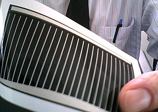
A copper indium gallium selenide solar cell is a thin-film solar cell used to convert sunlight into electric power. It is manufactured by depositing a thin layer of copper indium gallium selenide solution on glass or plastic backing, along with electrodes on the front and back to collect current. Because the material has a high absorption coefficient and strongly absorbs sunlight, a much thinner film is required than of other semiconductor materials.

Thermocompression bonding describes a wafer bonding technique and is also referred to as diffusion bonding, pressure joining, thermocompression welding or solid-state welding. Two metals, e.g. gold-gold (Au), are brought into atomic contact applying force and heat simultaneously. The diffusion requires atomic contact between the surfaces due to the atomic motion. The atoms migrate from one crystal lattice to the other one based on crystal lattice vibration. This atomic interaction sticks the interface together. The diffusion process is described by the following three processes:

Reactive multi-layer foils are a class of reactive materials, sometimes referred to as a pyrotechnic initiator of two mutually reactive metals, sputtered to form thin layers that create a laminated foil. On initiation by a heat pulse, delivered by a bridge wire, a laser pulse, an electric spark, a flame, or by other means, the metals undergo self-sustaining exothermic reaction, producing an intermetallic compound. The reaction occurs in solid and liquid phase only, without releasing any gas.

Direct bonding, or fusion bonding, describes a wafer bonding process without any additional intermediate layers. The bonding process is based on chemical bonds between two surfaces of any material possible meeting numerous requirements. These requirements are specified for the wafer surface as sufficiently clean, flat and smooth. Otherwise unbonded areas so called voids, i.e. interface bubbles, can occur.

Anodic bonding is a wafer bonding process to seal glass to either silicon or metal without introducing an intermediate layer; it is commonly used to seal glass to silicon wafers in electronics and microfluidics. This bonding technique, also known as field assisted bonding or electrostatic sealing, is mostly used for connecting silicon/glass and metal/glass through electric fields. The requirements for anodic bonding are clean and even wafer surfaces and atomic contact between the bonding substrates through a sufficiently powerful electrostatic field. Also necessary is the use of borosilicate glass containing a high concentration of alkali ions. The coefficient of thermal expansion (CTE) of the processed glass needs to be similar to those of the bonding partner.

Wafer bonding is a packaging technology on wafer-level for the fabrication of microelectromechanical systems (MEMS), nanoelectromechanical systems (NEMS), microelectronics and optoelectronics, ensuring a mechanically stable and hermetically sealed encapsulation. The wafers' diameter range from 100 mm to 200 mm for MEMS/NEMS and up to 300 mm for the production of microelectronic devices. Smaller wafers were used in the early days of the microelectronics industry, with wafers being just 1 inch in diameter in the 1950s.

Plasma-activated bonding is a derivative, directed to lower processing temperatures for direct bonding with hydrophilic surfaces. The main requirements for lowering temperatures of direct bonding are the use of materials melting at low temperatures and with different coefficients of thermal expansion (CTE).

<span class="mw-page-title-main">Eutectic bonding</span>

Eutectic bonding, also referred to as eutectic soldering, describes a wafer bonding technique with an intermediate metal layer that can produce a eutectic system. Those eutectic metals are alloys that transform directly from solid to liquid state, or vice versa from liquid to solid state, at a specific composition and temperature without passing a two-phase equilibrium, i.e. liquid and solid state. The fact that the eutectic temperature can be much lower than the melting temperature of the two or more pure elements can be important in eutectic bonding.

Glass frit bonding, also referred to as glass soldering or seal glass bonding, describes a wafer bonding technique with an intermediate glass layer. It is a widely used encapsulation technology for surface micro-machined structures, e.g., accelerometers or gyroscopes. This technique utilizes low melting-point glass and therefore provides various advantages including that viscosity of glass decreases with an increase of temperature. The viscous flow of glass has effects to compensate and planarize surface irregularities, convenient for bonding wafers with a high roughness due to plasma etching or deposition. A low viscosity promotes hermetically sealed encapsulation of structures based on a better adaption of the structured shapes. Further, the coefficient of thermal expansion (CTE) of the glass material is adapted to silicon. This results in low stress in the bonded wafer pair. The glass has to flow and wet the soldered surfaces well below the temperature where deformation or degradation of either of the joined materials or nearby structures occurs. The usual temperature of achieving flowing and wetting is between 450 and 550 °C.

Two dimensional hexagonal boron nitride is a material of comparable structure to graphene with potential applications in e.g. photonics., fuel cells and as a substrate for two-dimensional heterostructures. 2D h-BN is isostructural to graphene, but where graphene is conductive, 2D h-BN is a wide-gap insulator.

Glossary of microelectronics manufacturing terms

References

  1. 1 2 3 4 5 6 7 Böttge, B. and Bräuer, J. and Wiemer, M. and Petzold, M. and Bagdahn, J. and Gessner, T. (2010). "Fabrication and characterization of reactive nanoscale multilayer systems for low-temperature bonding in microsystem technology". Journal of Micromechanics and Microengineering. Vol. 20, no. 6.{{cite news}}: CS1 maint: multiple names: authors list (link)
  2. 1 2 3 4 5 6 7 8 9 Lin, Y.-C. and Baum, M. and Haubold, M. and Frömel, J. and Wiemer, M. and Gessner, T. and Esashi, M. (2009). "Development and evaluation of AuSi eutectic wafer bonding". Solid-State Sensors, Actuators and Microsystems Conference, 2009. TRANSDUCERS 2009. International. pp. 244–247. doi:10.1109/SENSOR.2009.5285519.{{cite conference}}: CS1 maint: multiple names: authors list (link)
  3. Qiu, X. & Wang, J. (2008). "Bonding silicon wafers with reactive multilayer foils". Sensors and Actuators A: Physical. 141 (2): 476–481. doi:10.1016/j.sna.2007.10.039.
  4. 1 2 3 4 5 6 Wiemer, M. and Bräuer, J. and Wünsch, D. and Gessner, T. (2010). "Reactive Bonding and Low Temperature Bonding of Heterogeneous Materials". ECS Transactions. 33 (4): 307–318. Bibcode:2010ECSTr..33d.307W. doi:10.1149/1.3483520. S2CID   96914667.{{cite journal}}: CS1 maint: multiple names: authors list (link)
  5. 1 2 Wang, J. and Besnoin, E. and Knio, O. M. and Weihs, T. P. (2004). "Investigating the effect of applied pressure on reactive multilayer foil joining". Acta Materialia. 52 (18): 5265–5274. Bibcode:2004AcMat..52.5265W. doi:10.1016/j.actamat.2004.07.012.{{cite journal}}: CS1 maint: multiple names: authors list (link)
  6. Qiu, X. and Welch, D. and Christen, J. and Zhu, J. and Oiler, J. and Yu, C. and Wang, Z. and Yu, H. (2010). "Reactive nanolayers for physiologically compatible microsystem packaging". Journal of Materials Science: Materials in Electronics. 21 (6): 562–566. doi:10.1007/s10854-009-9957-5. S2CID   137116832.{{cite journal}}: CS1 maint: multiple names: authors list (link)