
Microelectromechanical systems (MEMS), also written as micro-electro-mechanical systems and the related micromechatronics and microsystems constitute the technology of microscopic devices, particularly those with moving parts. They merge at the nanoscale into nanoelectromechanical systems (NEMS) and nanotechnology. MEMS are also referred to as micromachines in Japan and microsystem technology (MST) in Europe.
In integrated circuit manufacturing, photolithography or optical lithography is a general term used for techniques that use light to produce minutely patterned thin films of suitable materials over a substrate, such as a silicon wafer, to protect selected areas of it during subsequent etching, deposition, or implantation operations. Typically, ultraviolet light is used to transfer a geometric design from an optical mask to a light-sensitive chemical (photoresist) coated on the substrate. The photoresist either breaks down or hardens where it is exposed to light. The patterned film is then created by removing the softer parts of the coating with appropriate solvents.

Semiconductor device fabrication is the process used to manufacture semiconductor devices, typically integrated circuit (IC) chips such as modern computer processors, microcontrollers, and memory chips such as NAND flash and DRAM that are present in everyday electrical and electronic devices. It is a multiple-step sequence of photolithographic and chemical processing steps during which electronic circuits are gradually created on a wafer made of pure semiconducting material. Silicon is almost always used, but various compound semiconductors are used for specialized applications.
A semiconductor material has an electrical conductivity value falling between that of a conductor, such as metallic copper, and an insulator, such as glass. Its resistivity falls as its temperature rises; metals behave in the opposite way. Its conducting properties may be altered in useful ways by introducing impurities ("doping") into the crystal structure. When two differently doped regions exist in the same crystal, a semiconductor junction is created. The behavior of charge carriers, which include electrons, ions, and electron holes, at these junctions is the basis of diodes, transistors, and most modern electronics. Some examples of semiconductors are silicon, germanium, gallium arsenide, and elements near the so-called "metalloid staircase" on the periodic table. After silicon, gallium arsenide is the second-most common semiconductor and is used in laser diodes, solar cells, microwave-frequency integrated circuits, and others. Silicon is a critical element for fabricating most electronic circuits.
Reactive-ion etching (RIE) is an etching technology used in microfabrication. RIE is a type of dry etching which has different characteristics than wet etching. RIE uses chemically reactive plasma to remove material deposited on wafers. The plasma is generated under low pressure (vacuum) by an electromagnetic field. High-energy ions from the plasma attack the wafer surface and react with it.
Surface micromachining builds microstructures by deposition and etching structural layers over a substrate. This is different from Bulk micromachining, in which a silicon substrate wafer is selectively etched to produce structures.
Wafer fabrication is a procedure composed of many repeated sequential processes to produce complete electrical or photonic circuits on semiconductor wafers in semiconductor device fabrication process. Examples include production of radio frequency (RF) amplifiers, LEDs, optical computer components, and microprocessors for computers. Wafer fabrication is used to build components with the necessary electrical structures.

An ion beam is a type of charged particle beam consisting of ions. Ion beams have many uses in electronics manufacturing and other industries. A variety of ion beam sources exists, some derived from the mercury vapor thrusters developed by NASA in the 1960s. The most common ion beams are of singly-charged ions.
In semiconductor fabrication, a resist is a thin layer used to transfer a circuit pattern to the semiconductor substrate which it is deposited upon. A resist can be patterned via lithography to form a (sub)micrometer-scale, temporary mask that protects selected areas of the underlying substrate during subsequent processing steps. The material used to prepare said thin layer is typically a viscous solution. Resists are generally proprietary mixtures of a polymer or its precursor and other small molecules that have been specially formulated for a given lithography technology. Resists used during photolithography are called photoresists.
Deep reactive-ion etching (DRIE) is a highly anisotropic etch process used to create deep penetration, steep-sided holes and trenches in wafers/substrates, typically with high aspect ratios. It was developed for microelectromechanical systems (MEMS), which require these features, but is also used to excavate trenches for high-density capacitors for DRAM and more recently for creating through silicon vias (TSVs) in advanced 3D wafer level packaging technology. In DRIE, the substrate is placed inside a reactor, and several gases are introduced. A plasma is struck in the gas mixture which breaks the gas molecules into ions. The ions accelerated towards, and react with the surface of the material being etched, forming another gaseous element. This is known as the chemical part of the reactive ion etching. There is also a physical part, if ions have enough energy, they can knock atoms out of the material to be etched without chemical reaction.

Microfabrication is the process of fabricating miniature structures of micrometre scales and smaller. Historically, the earliest microfabrication processes were used for integrated circuit fabrication, also known as "semiconductor manufacturing" or "semiconductor device fabrication". In the last two decades microelectromechanical systems (MEMS), microsystems, micromachines and their subfields, microfluidics/lab-on-a-chip, optical MEMS, RF MEMS, PowerMEMS, BioMEMS and their extension into nanoscale have re-used, adapted or extended microfabrication methods. Flat-panel displays and solar cells are also using similar techniques.
Plasma etching is a form of plasma processing used to fabricate integrated circuits. It involves a high-speed stream of glow discharge (plasma) of an appropriate gas mixture being shot at a sample. The plasma source, known as etch species, can be either charged (ions) or neutral. During the process, the plasma generates volatile etch products at room temperature from the chemical reactions between the elements of the material etched and the reactive species generated by the plasma. Eventually the atoms of the shot element embed themselves at or just below the surface of the target, thus modifying the physical properties of the target.

Lam Research Corporation is an American supplier of wafer fabrication equipment and related services to the semiconductor industry. Its products are used primarily in front-end wafer processing, which involves the steps that create the active components of semiconductor devices and their wiring (interconnects). The company also builds equipment for back-end wafer-level packaging (WLP) and for related manufacturing markets such as for microelectromechanical systems (MEMS).
In semiconductor electronics fabrication technology, a self-aligned gate is a transistor manufacturing feature whereby the gate electrode of a MOSFET is used as a mask for the doping of the source and drain regions. This technique ensures that the gate is naturally and precisely aligned to the edges of the source and drain.

Etching is used in microfabrication to chemically remove layers from the surface of a wafer during manufacturing. Etching is a critically important process module, and every wafer undergoes many etching steps before it is complete.

ASM International is a Dutch headquartered multinational corporation that specializes in design, manufacturing, sales and service of semiconductor wafer processing equipment for the fabrication of semiconductor devices. ASM's products are used by semiconductor manufacturers in front-end wafer processing in their semiconductor fabrication plants. ASM’s technologies include atomic layer deposition, epitaxy, chemical vapor deposition and diffusion.

Veeco is a global capital equipment supplier, headquartered in the U.S., that designs and builds processing systems used in semiconductor and compound semiconductor manufacturing, data storage and scientific markets for applications such as advanced packaging, photonics, power electronics and display technologies.

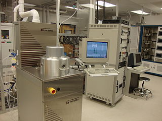
Tokyo Electron Limited, or TEL, is a Japanese electronics and semiconductor company headquartered in Akasaka, Minato-ku, Tokyo, Japan. The company was founded as Tokyo Electron Laboratories, Inc. in 1963.
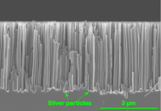
Metal Assisted Chemical Etching is the process of wet chemical etching of semiconductors with the use of a metal catalyst, usually deposited on the surface of a semiconductor in the form of a thin film or nanoparticles. The semiconductor, covered with the metal is then immersed in an etching solution containing and oxidizing agent and hydrofluoric acid. The metal on the surface catalyzes the reduction of the oxidizing agent and therefore in turn also the dissolution of silicon. In the majority of the conducted research this phenomenon of increased dissolution rate is also spatially confined, such that it is increased in close proximity to a metal particle at the surface. Eventually this leads to the formation of straight pores that are etched into the semiconductor. This means that a pre-defined pattern of the metal on the surface can be directly transferred to a semiconductor substrate.
Glossary of microelectronics manufacturing terms