This article includes a list of references, related reading, or external links, but its sources remain unclear because it lacks inline citations .(November 2017) |
General information | |
---|---|
Launched | 1995 |
Discontinued | 1997 |
Designed by | Sun Microsystems |
Performance | |
Max. CPU clock rate | 143 MHz to 200 MHz |
Architecture and classification | |
Instruction set | SPARC V9 |
Physical specifications | |
Cores |
|
History | |
Predecessor(s) | SuperSPARC II |
Successor(s) | UltraSPARC II |
The UltraSPARC is a microprocessor developed by Sun Microsystems and fabricated by Texas Instruments, introduced in mid-1995. It is the first microprocessor from Sun to implement the 64-bit SPARC V9 instruction set architecture (ISA). Marc Tremblay was a co-microarchitect.
The UltraSPARC is a four-issue superscalar microprocessor that executes instructions in in-order. It includes a nine-stage integer pipeline.
The execution units were simplified relative to the SuperSPARC to achieve higher clock frequencies - an example of a simplification is that the ALUs were not cascaded, unlike the SuperSPARC, to avoid restricting clock frequency.
The integer register file has 32 64-bit entries. As the SPARC ISA uses register windows, of which the UltraSPARC has eight, the actual number of registers is 144. The register file has seven read and three write ports. The integer register file provides registers to two arithmetic logic units and the load/store unit. The two ALUs can both execute arithmetic, logic and shift instructions but only one can execute multiply and divide instructions.
The floating-point unit consists of five functional units. One executes floating point adds and subtracts, one multiplies, one divides and square-roots. Two units are for executing SIMD instructions defined by the Visual Instruction Set (VIS). The floating-point register file contains thirty-two 64-bit registers. It has five read ports and three write ports.
The UltraSPARC has two levels of cache, primary and secondary. There are two primary caches, one for instructions and one for data. Both have a capacity of 16 KB.
The UltraSPARC required a mandatory external secondary cache. The cache is unified, has a capacity of 512 KB to 4 MB and is direct-mapped. It can return data in a single cycle. The external cache is implemented with synchronous SRAMs clocked at the same frequency as the microprocessor, as ratios were not supported. It is accessed via the data bus.
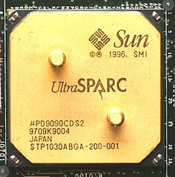
It contained 3.8 million transistors. It was fabricated in Texas Instruments' EPIC-3 process, a 0.5 μm complementary metal–oxide–semiconductor (CMOS) process with four levels of metal. The UltraSPARC was not fabricated in a BiCMOS process as Texas Instruments claimed it did not scale well to 0.5 μm processes and offered little performance improvement. The process was perfected on TI's MVP digital signal processor (DSP) with some features missing such as three levels of metal instead of four and a 0.55 feature size, before it was used to fabricate the UltraSPARC to avoid a repeat of the fabrication problems encountered with SuperSPARC.
The UltraSPARC is packaged in a 521-contact plastic ball grid array (PBGA).
The Pentium is a x86 microprocessor introduced by Intel on March 22, 1993. It is the first CPU using the Pentium brand. Considered the fifth generation in the 8086 compatible line of processors, its implementation and microarchitecture was internally called P5.
The POWER5 is a microprocessor developed and fabricated by IBM. It is an improved version of the POWER4. The principal improvements are support for simultaneous multithreading (SMT) and an on-die memory controller. The POWER5 is a dual-core microprocessor, with each core supporting one physical thread and two logical threads, for a total of two physical threads and four logical threads.
SPARC64 is a microprocessor developed by HAL Computer Systems and fabricated by Fujitsu. It implements the SPARC V9 instruction set architecture (ISA), the first microprocessor to do so. SPARC64 was HAL's first microprocessor and was the first in the SPARC64 brand. It operates at 101 and 118 MHz. The SPARC64 was used exclusively by Fujitsu in their systems; the first systems, the Fujitsu HALstation Model 330 and Model 350 workstations, were formally announced in September 1995 and were introduced in October 1995, two years late. It was succeeded by the SPARC64 II in 1996.
The POWER3 is a microprocessor, designed and exclusively manufactured by IBM, that implemented the 64-bit version of the PowerPC instruction set architecture (ISA), including all of the optional instructions of the ISA such as instructions present in the POWER2 version of the POWER ISA but not in the PowerPC ISA. It was introduced on 5 October 1998, debuting in the RS/6000 43P Model 260, a high-end graphics workstation. The POWER3 was originally supposed to be called the PowerPC 630 but was renamed, probably to differentiate the server-oriented POWER processors it replaced from the more consumer-oriented 32-bit PowerPCs. The POWER3 was the successor of the P2SC derivative of the POWER2 and completed IBM's long-delayed transition from POWER to PowerPC, which was originally scheduled to conclude in 1995. The POWER3 was used in IBM RS/6000 servers and workstations at 200 MHz. It competed with the Digital Equipment Corporation (DEC) Alpha 21264 and the Hewlett-Packard (HP) PA-8500.
The CVAX is a microprocessor chipset developed and fabricated by Digital Equipment Corporation (DEC) that implemented the VAX instruction set architecture (ISA). The chipset consisted of the CVAX 78034 CPU, CFPA floating-point accelerator, CVAX clock chip, and the associated support chips, the CVAX System Support Chip (CSSC), CVAX Memory Controller (CMCTL), and CVAX Q-Bus Interface Chip (CQBIC).
The R10000, code-named "T5", is a RISC microprocessor implementation of the MIPS IV instruction set architecture (ISA) developed by MIPS Technologies, Inc. (MTI), then a division of Silicon Graphics, Inc. (SGI). The chief designers are Chris Rowen and Kenneth C. Yeager. The R10000 microarchitecture is known as ANDES, an abbreviation for Architecture with Non-sequential Dynamic Execution Scheduling. The R10000 largely replaces the R8000 in the high-end and the R4400 elsewhere. MTI was a fabless semiconductor company; the R10000 was fabricated by NEC and Toshiba. Previous fabricators of MIPS microprocessors such as Integrated Device Technology (IDT) and three others did not fabricate the R10000 as it was more expensive to do so than the R4000 and R4400.
The R4000 is a microprocessor developed by MIPS Computer Systems that implements the MIPS III instruction set architecture (ISA). Officially announced on 1 October 1991, it was one of the first 64-bit microprocessors and the first MIPS III implementation. In the early 1990s, when RISC microprocessors were expected to replace CISC microprocessors such as the Intel i486, the R4000 was selected to be the microprocessor of the Advanced Computing Environment (ACE), an industry standard that intended to define a common RISC platform. ACE ultimately failed for a number of reasons, but the R4000 found success in the workstation and server markets.
The R5000 is a 64-bit, bi-endian, superscalar, in-order execution 2-issue design microprocessor, that implements the MIPS IV instruction set architecture (ISA) developed by Quantum Effect Design (QED) in 1996. The project was funded by MIPS Technologies, Inc (MTI), also the licensor. MTI then licensed the design to Integrated Device Technology (IDT), NEC, NKK, and Toshiba. The R5000 succeeded the QED R4600 and R4700 as their flagship high-end embedded microprocessor. IDT marketed its version of the R5000 as the 79RV5000, NEC as VR5000, NKK as the NR5000, and Toshiba as the TX5000. The R5000 was sold to PMC-Sierra when the company acquired QED. Derivatives of the R5000 are still in production today for embedded systems.
The R8000 is a microprocessor chipset developed by MIPS Technologies, Inc. (MTI), Toshiba, and Weitek. It was the first implementation of the MIPS IV instruction set architecture. The R8000 is also known as the TFP, for Tremendous Floating-Point, its name during development.
The POWER2, originally named RIOS2, is a processor designed by IBM that implemented the POWER instruction set architecture. The POWER2 was the successor of the POWER1, debuting in September 1993 within IBM's RS/6000 systems. When introduced, the POWER2 was the fastest microprocessor, surpassing the Alpha 21064. When the Alpha 21064A was introduced in 1993, the POWER2 lost the lead and became second. IBM claimed that the performance for a 62.5 MHz POWER2 was 73.3 SPECint92 and 134.6 SPECfp92.
The Alpha 21064 is a microprocessor developed and fabricated by Digital Equipment Corporation that implemented the Alpha instruction set architecture (ISA). It was introduced as the DECchip 21064 before it was renamed in 1994. The 21064 is also known by its code name, EV4. It was announced in February 1992 with volume availability in September 1992. The 21064 was the first commercial implementation of the Alpha ISA, and the first microprocessor from Digital to be available commercially. It was succeeded by a derivative, the Alpha 21064A in October 1993. This last version was replaced by the Alpha 21164 in 1995.
The Alpha 21164, also known by its code name, EV5, is a microprocessor developed and fabricated by Digital Equipment Corporation that implemented the Alpha instruction set architecture (ISA). It was introduced in January 1995, succeeding the Alpha 21064A as Digital's flagship microprocessor. It was succeeded by the Alpha 21264 in 1998.
The Alpha 21264 is a Digital Equipment Corporation RISC microprocessor launched on 19 October 1998. The 21264 implemented the Alpha instruction set architecture (ISA).
The SPARC64 V (Zeus) is a SPARC V9 microprocessor designed by Fujitsu. The SPARC64 V was the basis for a series of successive processors designed for servers, and later, supercomputers.
The hyperSPARC, code-named "Pinnacle", is a microprocessor that implements the SPARC Version 8 instruction set architecture (ISA) developed by Ross Technology for Cypress Semiconductor.
The PA-8000 (PCX-U), code-named Onyx, is a microprocessor developed and fabricated by Hewlett-Packard (HP) that implemented the PA-RISC 2.0 instruction set architecture (ISA). It was a completely new design with no circuitry derived from previous PA-RISC microprocessors. The PA-8000 was introduced on 2 November 1995 when shipments began to members of the Precision RISC Organization (PRO). It was used exclusively by PRO members and was not sold on the merchant market. All follow-on PA-8x00 processors are based on the basic PA-8000 processor core.
The UltraSPARC III, code-named "Cheetah", is a microprocessor that implements the SPARC V9 instruction set architecture (ISA) developed by Sun Microsystems and fabricated by Texas Instruments. It was introduced in 2001 and operates at 600 to 900 MHz. It was succeeded by the UltraSPARC IV in 2004. Gary Lauterbach was the chief architect.
The TurboSPARC is a microprocessor that implements the SPARC V8 instruction set architecture (ISA) developed by Fujitsu Microelectronics, Inc. (FMI), the United States subsidiary of the Japanese multinational information technology equipment and services company Fujitsu Limited located in San Jose, California. It was a low-end microprocessor primarily developed as an upgrade for the Sun Microsystems microSPARC-II-based SPARCstation 5 workstation. It was introduced on 30 September 1996, with a 170 MHz version priced at US$499 in quantities of 1,000. The TurboSPARC was mostly succeeded in the low-end SPARC market by the UltraSPARC IIi in late 1997, but remained available.
The PA-7100LC is a microprocessor that implements the PA-RISC 1.1 instruction set architecture (ISA) developed by Hewlett-Packard (HP). It is also known as the PCX-L, and by its code-name, Hummingbird. It was designed as a low-cost microprocessor for low-end systems. The first systems to feature the PA-7100LC were introduced in January 1994. These systems used 60 and 80 MHz parts. A 100 MHz part debuted in June 1994. The PA-7100LC was the first PA-RISC microprocessor to implement the MAX-1 multimedia instructions, an early single instruction, multiple data (SIMD) multimedia instruction set extension that provided instructions for improving the performance of MPEG video decoding.
The R4600, code-named "Orion", is a microprocessor developed by Quantum Effect Design (QED) that implemented the MIPS III instruction set architecture (ISA). As QED was a design firm that did not fabricate or sell their designs, the R4600 was first licensed to Integrated Device Technology (IDT), and later to Toshiba and then NKK. These companies fabricated the microprocessor and marketed it. The R4600 was designed as a low-end workstation or high-end embedded microprocessor. Users included Silicon Graphics, Inc. (SGI) for their Indy workstation and DeskStation Technology for their Windows NT workstations. The R4600 was instrumental in making the Indy successful by providing good integer performance at a competitive price. In embedded systems, prominent users included Cisco Systems in their network routers and Canon in their printers.