General information | |
---|---|
Launched | 2013 |
Discontinued | 2017 |
Performance | |
Max. CPU clock rate | 3.6 GHz |
Cache | |
L1 cache | 16×(16+16) KB |
L2 cache | 16×128 KB |
L3 cache | 8 MB |
Architecture and classification | |
Technology node | 28 nm |
Instruction set | SPARC V9 |
Physical specifications | |
Cores |
|
Products, models, variants | |
Core name(s) |
|
History | |
Predecessor(s) | SPARC T4 |
Successor(s) | SPARC M7 |
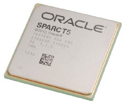
SPARC T5 is the fifth generation multicore microprocessor of Oracle's SPARC T series family. [1] It was first presented at Hot Chips 24 in August 2012, [2] and was officially introduced with the Oracle SPARC T5 servers in March 2013. [3] The processor is designed to offer high multithreaded performance (16 cores per chip, with 8 threads per core), as well as high single threaded performance from the same chip. [4]
The processor uses the same SPARC S3 core design as its predecessor, the SPARC T4 processor, but is implemented in a 28 nm process and runs at 3.6 GHz. [5] The S3 core is a dual-issue core that uses dynamic threading and out-of-order execution, [6] incorporates one floating point unit, one dedicated cryptographic unit per core. [7]
The 64-bit SPARC Version 9 based processor has 16 cores supporting up to 128 threads per processor, and scales up to 1,024 threads in an 8 socket system. [4] Other changes include the support of PCIe version 3.0 and a new cache coherence protocol. [5]
This chart shows some differences between the T5 and T4 processor chips.
Processor | SPARC T4 [4] | SPARC T5 [8] | T7 / M7 [9] |
---|---|---|---|
Max chips per system | 4 | 8 | 16 |
Cores per chip | 8 | 16 | 32 |
Max threads per chip | 64 | 128 | 256 |
Frequency | 2.85–3.0 GHz | 3.6 GHz | 4.13 GHz |
Shared Level 3 cache | 4 MB | 8 MB | 64 MB |
MCUs per chip | 2 [10] | 4 [11] | 4 |
Transfer rate per MCU | 6.4 Gbit/s [10] | 12.8 Gbit/s [11] | |
Process Technology | 40 nm | 28 nm | 20 nm |
Die size | 403 mm2 | 478 mm2 | |
PCIe Version | 2.0 | 3.0 | 3.0 |
The SPARC T5 also introduces a new power management feature that consists of hardware support in the processor, and the software that allows system administrator to use the feature. Users select the policy how the system responds to over-temperature and over-current events. The dynamic voltage and frequency scaling (aka DVFS) policy can be set to maintain peak frequency, or to trade off between performance and power consumption. [5]
The SPARC T5 processor is used in Oracle's entry and mid-size SPARC T5-2, T5-4, and T5-8 servers. All servers use the same processor frequency, number of cores per chip and cache configuration. [12]
The T5 processor includes a crossbar network that connects the 16 cores with the L2 caches to the shared L3 cache. Multiprocessor cache coherence is maintained using a directory-based protocol. [5] The design scales up to eight sockets without additional silicon (glueless). The snooping based protocol used in SPARC T4 systems was replaced in order to reduce memory latency and reduce coherency bandwidth consumption. [5] [13]
Itanium is a discontinued family of 64-bit Intel microprocessors that implement the Intel Itanium architecture. The Itanium architecture originated at Hewlett-Packard (HP), and was later jointly developed by HP and Intel. Launched in June 2001, Intel initially marketed the processors for enterprise servers and high-performance computing systems. In the concept phase, engineers said "we could run circles around PowerPC...we could kill the x86." Early predictions were that IA-64 would expand to the lower-end servers, supplanting Xeon, and eventually penetrate into the personal computers, eventually to supplant reduced instruction set computing (RISC) and complex instruction set computing (CISC) architectures for all general-purpose applications.
SPARC is a reduced instruction set computer (RISC) instruction set architecture originally developed by Sun Microsystems. Its design was strongly influenced by the experimental Berkeley RISC system developed in the early 1980s. First developed in 1986 and released in 1987, SPARC was one of the most successful early commercial RISC systems, and its success led to the introduction of similar RISC designs from many vendors through the 1980s and 1990s.
Simultaneous multithreading (SMT) is a technique for improving the overall efficiency of superscalar CPUs with hardware multithreading. SMT permits multiple independent threads of execution to better use the resources provided by modern processor architectures.
POWER7 is a family of superscalar multi-core microprocessors based on the Power ISA 2.06 instruction set architecture released in 2010 that succeeded the POWER6 and POWER6+. POWER7 was developed by IBM at several sites including IBM's Rochester, MN; Austin, TX; Essex Junction, VT; T. J. Watson Research Center, NY; Bromont, QC and IBM Deutschland Research & Development GmbH, Böblingen, Germany laboratories. IBM announced servers based on POWER7 on 8 February 2010.
Sun Microsystems' UltraSPARC T1 microprocessor, known until its 14 November 2005 announcement by its development codename "Niagara", is a multithreading, multicore CPU. Designed to lower the energy consumption of server computers, the CPU typically uses 72 W of power at 1.4 GHz.
A multi-core processor is a microprocessor on a single integrated circuit with two or more separate processing units, called cores, each of which reads and executes program instructions. The instructions are ordinary CPU instructions but the single processor can run instructions on separate cores at the same time, increasing overall speed for programs that support multithreading or other parallel computing techniques. Manufacturers typically integrate the cores onto a single integrated circuit die or onto multiple dies in a single chip package. The microprocessors currently used in almost all personal computers are multi-core.
Rock was a multithreading, multicore, SPARC microprocessor under development at Sun Microsystems. Canceled in 2010, it was a separate project from the SPARC T-Series (CoolThreads/Niagara) family of processors.
The UltraSPARC IVJaguar and follow-up UltraSPARC IV+Panther are microprocessors designed by Sun Microsystems and manufactured by Texas Instruments. They are the fourth generation of UltraSPARC microprocessors, and implement the 64-bit SPARC V9 instruction set architecture (ISA). The UltraSPARC IV was originally to be succeeded by the UltraSPARC V Millennium, which was canceled after the announcement of the Niagara, now UltraSPARC T1 microprocessor in early 2004. It was instead succeeded by the Fujitsu-designed SPARC64 VI.
Sun Microsystems' UltraSPARC T2 microprocessor is a multithreading, multi-core CPU. It is a member of the SPARC family, and the successor to the UltraSPARC T1. The chip is sometimes referred to by its codename, Niagara 2. Sun started selling servers with the T2 processor in October 2007.
Logical Domains is the server virtualization and partitioning technology for SPARC V9 processors. It was first released by Sun Microsystems in April 2007. After the Oracle acquisition of Sun in January 2010, the product has been re-branded as Oracle VM Server for SPARC from version 2.0 onwards.
The SPARC Enterprise series is a range of UNIX server computers based on the SPARC V9 architecture. It was co-developed by Sun Microsystems and Fujitsu, announced on June 1, 2004, and introduced in 2007. They were marketed and sold by Sun Microsystems, Fujitsu, and Fujitsu Siemens Computers under the common brand of "SPARC Enterprise", superseding Sun's Sun Fire and Fujitsu's PRIMEPOWER server product lines. Codename is APL.
The SPARC64 V (Zeus) is a SPARC V9 microprocessor designed by Fujitsu. The SPARC64 V was the basis for a series of successive processors designed for servers, and later, supercomputers.
Afara Websystems Inc. was a Sunnyvale, California, USA server company whose goal was to build servers surrounding a custom high-throughput CPU architecture, "developing IP traffic management systems that will bring quality-of-service to the next generation of IP access infrastructure." The word "Afara" means "bridge" in the West African Yoruba language.
The SPARC T3 microprocessor is a multithreading, multi-core CPU produced by Oracle Corporation. Officially launched on 20 September 2010, it is a member of the SPARC family, and the successor to the UltraSPARC T2.
Oyekunle Ayinde "Kunle" Olukotun is a British-born Nigerian computer scientist who is the Cadence Design Systems Professor of the Stanford School of Engineering, Professor of Electrical Engineering and Computer Science at Stanford University and the director of the Stanford Pervasive Parallelism Lab. Olukotun is known as the “father of the multi-core processor”, and the leader of the Stanford Hydra Chip Multiprocessor research project. Olukotun's achievements include designing the first general-purpose multi-core CPU, innovating single-chip multiprocessor and multi-threaded processor design, and pioneering multicore CPUs and GPUs, transactional memory technology and domain-specific languages programming models. Olukotun's research interests include computer architecture, parallel programming environments and scalable parallel systems, domain specific languages and high-level compilers.
The SPARC T4 is a SPARC multicore microprocessor introduced in 2011 by Oracle Corporation. The processor is designed to offer high multithreaded performance, as well as high single threaded performance from the same chip. The chip is the 4th generation processor in the T-Series family. Sun Microsystems brought the first T-Series processor to market in 2005.
The SPARC T-series family of RISC processors and server computers, based on the SPARC V9 architecture, was originally developed by Sun Microsystems, and later by Oracle Corporation after its acquisition of Sun. Its distinguishing feature from earlier SPARC iterations is the introduction of chip multithreading (CMT) technology, a multithreading, multicore design intended to drive greater processor utilization at lower power consumption.
POWER9 is a family of superscalar, multithreading, multi-core microprocessors produced by IBM, based on the Power ISA. It was announced in August 2016. The POWER9-based processors are being manufactured using a 14 nm FinFET process, in 12- and 24-core versions, for scale out and scale up applications, and possibly other variations, since the POWER9 architecture is open for licensing and modification by the OpenPOWER Foundation members.
Ampere Computing LLC is an American fabless semiconductor company based in Santa Clara, California that develops processors for servers operating in large scale environments. Ampere also has offices in: Portland, Oregon; Taipei, Taiwan; Raleigh, North Carolina; Bangalore, India; Warsaw, Poland; and Ho Chi Minh City, Vietnam.