Optical contact bonding is a glueless process whereby two closely conformal surfaces are joined, being held purely by intermolecular forces.
Optical contact bonding is a glueless process whereby two closely conformal surfaces are joined, being held purely by intermolecular forces.
Isaac Newton has been credited with the first description of conformal interaction observed through the interference phenomenon known as Newton's rings, though it was S. D. Poisson in 1823 who first described the optical characteristics of two identical surfaces in contact. It was not until the 19th century that objects were made with such precision that the binding phenomenon was observed. The bond was referred to as "ansprengen" in German language.
By 1900, optical contact bonding was being employed in the construction of optical prisms, and the following century saw further research into the phenomenon at the same time that ideas of inter-atom interactions were first being studied. [1]
Intermolecular forces such as Van der Waals forces, hydrogen bonds, and dipole–dipole interactions are typically not sufficiently strong to hold two apparently conformal rigid bodies together, since the forces drop off rapidly with distance, [2] and the actual area in contact between the two bodies is small due to surface roughness and minor imperfections.
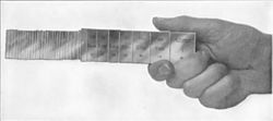
However, if the bodies are conformal to an accuracy of better than 10 angstroms (1 nanometer), then a sufficient surface area is in close enough contact for the intermolecular interactions to have an observable macroscopic effect—that is, the two objects stick together. [3] Such a condition requires a high degree of accuracy and surface smoothness, which is typically found in optical components, such as prisms.
In addition to both surfaces' being practically conformal (in practice often completely flat), the surfaces must also be extremely clean and free from any small contamination that would prevent or weaken the bond—including grease films and specks of dust. [4] For bonding to occur, the surfaces need only to be brought together; the intermolecular forces draw the bodies into the lowest energy conformation, and no pressure needs to be applied.
Since the method requires no binder, balsam or glue, the physical properties of the bound object are the same as the objects joined. Typically, glues and binders are more heat sensitive or have undesirable properties compared to the actual bodies being joined. The use of optical contact bonding allows the production of a final product with properties as well as the bulk solid. [5] This can include temperature and chemical resistances, spectral absorption properties and reduced contamination from bonding materials.
| | This section needs expansion. You can help by adding to it. (December 2009) |
Since the early 20th Century, optical contact bonding has been most widely used in the fabrication of compound optical components, such as cube beam splitters and prism assemblies, where two or more precisely polished glass elements are joined without adhesives. [4] [6] [7] Optical contact bonding eliminates refractive-index discontinuities and absorption losses from adhesives, impurities, or air gaps that would otherwise degrade optical performance, making it particularly valuable in interferometry and precision imaging systems. [6] The technique is also used in high-power laser optics. Adhesive layers can absorb laser radiation, thermally degrade, or outgas, meaning optically contacted components exhibit higher laser-damage thresholds and improved thermal stability. [7] [8]
In optical metrology, contacting is used to assemble reference optics such as optical flats, etalons, and spacers, where long-term dimensional stability and sub-nanometre surface continuity are required for interferometric measurements. [6] [9] A closely related application is in semiconductor manufacturing, where optical contacting is essential for the direct wafer bonding techniques used in silicon-on-insulator (SOI) wafers and micro-electromechanical systems (MEMS). Here, atomically flat, clean surfaces can be further strengthened by thermal annealing. [10] [11]
Optical contact bonding is also used in vacum, space, and cryogenic systems, such as space telescopes and ultra-high-vacuum instrumentation, where organic bonding agents would risk outgassing, therefore ensuring mechanical stability across wide temperature and pressure ranges. [8] [9]
{{cite book}}: CS1 maint: location (link)