
Chemical vapor deposition (CVD) is a vacuum deposition method used to produce high quality, and high-performance, solid materials. The process is often used in the semiconductor industry to produce thin films.

MEMS is the technology of microscopic devices incorporating both electronic and moving parts. MEMS are made up of components between 1 and 100 micrometers in size, and MEMS devices generally range in size from 20 micrometres to a millimetre, although components arranged in arrays can be more than 1000 mm2. They usually consist of a central unit that processes data and several components that interact with the surroundings.
Silicon is a chemical element with the symbol Si and atomic number 14. It is a hard, brittle crystalline solid with a blue-grey metallic luster, and is a tetravalent metalloid and semiconductor. It is a member of group 14 in the periodic table: carbon is above it; and germanium, tin, lead, and flerovium are below it. It is relatively unreactive.

Semiconductor device fabrication is the process used to manufacture semiconductor devices, typically integrated circuits (ICs) such as computer processors, microcontrollers, and memory chips that are present in everyday electrical and electronic devices. It is a multiple-step photolithographic and physico-chemical process during which electronic circuits are gradually created on a wafer, typically made of pure single-crystal semiconducting material. Silicon is almost always used, but various compound semiconductors are used for specialized applications.
A semiconductor is a material which has an electrical conductivity value falling between that of a conductor, such as copper, and an insulator, such as glass. Its resistivity falls as its temperature rises; metals behave in the opposite way. Its conducting properties may be altered in useful ways by introducing impurities ("doping") into the crystal structure. When two differently doped regions exist in the same crystal, a semiconductor junction is created. The behavior of charge carriers, which include electrons, ions, and electron holes, at these junctions is the basis of diodes, transistors, and most modern electronics. Some examples of semiconductors are silicon, germanium, gallium arsenide, and elements near the so-called "metalloid staircase" on the periodic table. After silicon, gallium arsenide is the second-most common semiconductor and is used in laser diodes, solar cells, microwave-frequency integrated circuits, and others. Silicon is a critical element for fabricating most electronic circuits.

The metal–oxide–semiconductor field-effect transistor is a type of field-effect transistor (FET), most commonly fabricated by the controlled oxidation of silicon. It has an insulated gate, the voltage of which determines the conductivity of the device. This ability to change conductivity with the amount of applied voltage can be used for amplifying or switching electronic signals. A metal-insulator-semiconductor field-effect transistor (MISFET) is a term almost synonymous with MOSFET. Another synonym is IGFET for insulated-gate field-effect transistor.

Epitaxy refers to a type of crystal growth or material deposition in which new crystalline layers are formed with one or more well-defined orientations with respect to the crystalline seed layer. The deposited crystalline film is called an epitaxial film or epitaxial layer. The relative orientation(s) of the epitaxial layer to the seed layer is defined in terms of the orientation of the crystal lattice of each material. For most epitaxial growths, the new layer is usually crystalline and each crystallographic domain of the overlayer must have a well-defined orientation relative to the substrate crystal structure. Epitaxy can involve single-crystal structures, although grain-to-grain epitaxy has been observed in granular films. For most technological applications, single domain epitaxy, which is the growth of an overlayer crystal with one well-defined orientation with respect to the substrate crystal, is preferred. Epitaxy can also play an important role while growing superlattice structures.
A silicide is a type of chemical compound that combines silicon and a usually more electropositive element.
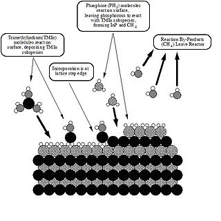
Metalorganic vapour-phase epitaxy (MOVPE), also known as organometallic vapour-phase epitaxy (OMVPE) or metalorganic chemical vapour deposition (MOCVD), is a chemical vapour deposition method used to produce single- or polycrystalline thin films. It is a process for growing crystalline layers to create complex semiconductor multilayer structures. In contrast to molecular-beam epitaxy (MBE), the growth of crystals is by chemical reaction and not physical deposition. This takes place not in vacuum, but from the gas phase at moderate pressures. As such, this technique is preferred for the formation of devices incorporating thermodynamically metastable alloys, and it has become a major process in the manufacture of optoelectronics, such as Light-emitting diodes. It was invented in 1968 at North American Aviation Science Center by Harold M. Manasevit.

Platinum silicide, also known as platinum monosilicide, is the inorganic compound with the formula PtSi. It is a semiconductor that turns into a superconductor when cooled to 0.8 K.
An ohmic contact is a non-rectifying electrical junction: a junction between two conductors that has a linear current–voltage (I–V) curve as with Ohm's law. Low-resistance ohmic contacts are used to allow charge to flow easily in both directions between the two conductors, without blocking due to rectification or excess power dissipation due to voltage thresholds.
In semiconductor electronics fabrication technology, a self-aligned gate is a transistor manufacturing approach whereby the gate electrode of a MOSFET is used as a mask for the doping of the source and drain regions. This technique ensures that the gate is naturally and precisely aligned to the edges of the source and drain.

A metal gate, in the context of a lateral metal–oxide–semiconductor (MOS) stack, is the gate electrode separated by an oxide from the transistor's channel – the gate material is made from a metal. In most MOS transistors since about the mid 1970s, the "M" for metal has been replaced by a non-metal gate material.

Veeco is a global capital equipment supplier, headquartered in the U.S., that designs and builds processing systems used in semiconductor and compound semiconductor manufacturing, data storage and scientific markets for applications such as advanced packaging, photonics, power electronics and display technologies.
Ultra-high-purity steam, also called the clean steam, UHP steam or high purity water vapor, is used in a variety of industrial manufacturing processes that require oxidation or annealing. These processes include the growth of oxide layers on silicon wafers for the semiconductor industry, originally described by the Deal-Grove model, and for the formation of passivation layers used to improve the light capture ability of crystalline photovoltaic cells. Several methods and technologies can be employed to generate ultra high purity steam, including pyrolysis, bubbling, direct liquid injection, and purified steam generation. The level of purity, or the relative lack of contamination, affects the quality of the oxide layer or annealed surface. The method of delivery affects growth rate, uniformity, and electrical performance. Oxidation and annealing are common steps in the manufacture of such devices as microelectronics and solar cells.
Direct bonding, or fusion bonding, describes a wafer bonding process without any additional intermediate layers. The bonding process is based on chemical bonds between two surfaces of any material possible meeting numerous requirements. These requirements are specified for the wafer surface as sufficiently clean, flat and smooth. Otherwise unbonded areas so called voids, i.e. interface bubbles, can occur.

Polycrystalline silicon, or multicrystalline silicon, also called polysilicon, poly-Si, or mc-Si, is a high purity, polycrystalline form of silicon, used as a raw material by the solar photovoltaic and electronics industry.
Eutectic bonding, also referred to as eutectic soldering, describes a wafer bonding technique with an intermediate metal layer that can produce a eutectic system. Those eutectic metals are alloys that transform directly from solid to liquid state, or vice versa from liquid to solid state, at a specific composition and temperature without passing a two-phase equilibrium, i.e. liquid and solid state. The fact that the eutectic temperature can be much lower than the melting temperature of the two or more pure elements can be important in eutectic bonding.

Binary compounds of silicon are binary chemical compounds containing silicon and one other chemical element. Technically the term silicide is reserved for any compounds containing silicon bonded to a more electropositive element. Binary silicon compounds can be grouped into several classes. Saltlike silicides are formed with the electropositive s-block metals. Covalent silicides and silicon compounds occur with hydrogen and the elements in groups 10 to 17.

Nickel silicides include several intermetallic compounds of nickel and silicon. Nickel silicides are important in microelectronics as they form at junctions of nickel and silicon. Additionally thin layers of nickel silicides may have application in imparting surface resistance to nickel alloys.
