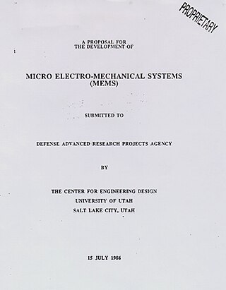
MEMS is the technology of microscopic devices incorporating both electronic and moving parts. MEMS are made up of components between 1 and 100 micrometres in size, and MEMS devices generally range in size from 20 micrometres to a millimetre, although components arranged in arrays can be more than 1000 mm2. They usually consist of a central unit that processes data and several components that interact with the surroundings.

Semiconductor device fabrication is the process used to manufacture semiconductor devices, typically integrated circuits (ICs) such as computer processors, microcontrollers, and memory chips that are present in everyday electronic devices. It is a multiple-step photolithographic and physio-chemical process during which electronic circuits are gradually created on a wafer, typically made of pure single-crystal semiconducting material. Silicon is almost always used, but various compound semiconductors are used for specialized applications.
Silicon on sapphire (SOS) is a hetero-epitaxial process for metal–oxide–semiconductor (MOS) integrated circuit (IC) manufacturing that consists of a thin layer of silicon grown on a sapphire wafer. SOS is part of the silicon-on-insulator (SOI) family of CMOS technologies.
Surface micromachining builds microstructures by deposition and etching structural layers over a substrate. This is different from Bulk micromachining, in which a silicon substrate wafer is selectively etched to produce structures.
A thin-film bulk acoustic resonator is a device consisting of a piezoelectric material manufactured by thin film methods between two conductive – typically metallic – electrodes and acoustically isolated from the surrounding medium. The operation is based on the piezoelectricity of the piezolayer between the electrodes.
Acoustic waves emitted by ultrasonics transducer crystals exhibit a property known as self-focusing. Note that this is distinct from the electronically controlled focusing employed in diagnostic ultrasound devices which employ arrays of transducers. The self-focusing effect exists even for a single crystal.
A hybrid silicon laser is a semiconductor laser fabricated from both silicon and group III-V semiconductor materials. The hybrid silicon laser was developed to address the lack of a silicon laser to enable fabrication of low-cost, mass-producible silicon optical devices. The hybrid approach takes advantage of the light-emitting properties of III-V semiconductor materials combined with the process maturity of silicon to fabricate electrically driven lasers on a silicon wafer that can be integrated with other silicon photonic devices.
D. Jackson Coleman is a professor of clinical ophthalmology at NewYork-Presbyterian Hospital at The Edward S. Harkness Eye Institute of Columbia University. He is the former John Milton McLean Professor of Ophthalmology and chairman emeritus at Weill Cornell Medical Center where he served as chairman from 1979 to 2006. His specialties are retinal diseases and ultrasound, working with patients at Columbia University Medical Center. Coleman is also engaged in research involving ultrasound, which he has pursued throughout his career with colleague Ronald Silverman in the Department of Ophthalmology at the Columbia University Medical Center.

Ultrasonic transducers and ultrasonic sensors are devices that generate or sense ultrasound energy. They can be divided into three broad categories: transmitters, receivers and transceivers. Transmitters convert electrical signals into ultrasound, receivers convert ultrasound into electrical signals, and transceivers can both transmit and receive ultrasound.

A radio-frequency microelectromechanical system is a microelectromechanical system with electronic components comprising moving sub-millimeter-sized parts that provide radio-frequency (RF) functionality. RF functionality can be implemented using a variety of RF technologies. Besides RF MEMS technology, III-V compound semiconductor, ferrite, ferroelectric, silicon-based semiconductor, and vacuum tube technology are available to the RF designer. Each of the RF technologies offers a distinct trade-off between cost, frequency, gain, large-scale integration, lifetime, linearity, noise figure, packaging, power handling, power consumption, reliability, ruggedness, size, supply voltage, switching time and weight.

Integrated passive devices (IPDs), also known as integrated passive components (IPCs) or embedded passive components (EPC), are electronic components where resistors (R), capacitors (C), inductors (L)/coils/chokes, microstriplines, impedance matching elements, baluns or any combinations of them are integrated in the same package or on the same substrate. Sometimes integrated passives can also be called as embedded passives, and still the difference between integrated and embedded passives is technically unclear. In both cases passives are realized in between dielectric layers or on the same substrate.

Schlieren imaging is a method to visualize density variations in transparent media.
The wafer bond characterization is based on different methods and tests. Considered a high importance of the wafer are the successful bonded wafers without flaws. Those flaws can be caused by void formation in the interface due to unevenness or impurities. The bond connection is characterized for wafer bond development or quality assessment of fabricated wafers and sensors.
Microelectromechanical system oscillators are devices that generate highly stable reference frequencies used to sequence electronic systems, manage data transfer, define radio frequencies, and measure elapsed time. The core technologies used in MEMS oscillators have been in development since the mid-1960s, but have only been sufficiently advanced for commercial applications since 2006. MEMS oscillators incorporate MEMS resonators, which are microelectromechanical structures that define stable frequencies. MEMS clock generators are MEMS timing devices with multiple outputs for systems that need more than a single reference frequency. MEMS oscillators are a valid alternative to older, more established quartz crystal oscillators, offering better resilience against vibration and mechanical shock, and reliability with respect to temperature variation.
Piezoelectric Micromachined Ultrasonic Transducers (PMUT) are MEMS-based piezoelectric ultrasonic transducers. Unlike bulk piezoelectric transducers which use the thickness-mode motion of a plate of piezoelectric ceramic such as PZT or single-crystal PMN-PT, PMUT are based on the flexural motion of a thin membrane coupled with a thin piezoelectric film, such as PVDF. In comparison with bulk piezoelectric ultrasound transducers, PMUT can offer advantages such as increased bandwidth, flexible geometries, natural acoustic impedance match with water, reduced voltage requirements, mixing of different resonant frequencies and potential for integration with supporting electronic circuits especially for miniaturized high frequency applications.
Ultrasonic antifouling is a technology that uses high frequency sound (ultrasound) to prevent or reduce biofouling on underwater structures, surfaces, and medium. Ultrasound is just high frequency sound. Ultrasound has the same physical properties as human-audible sound. The method has two primary forms: sub-cavitation intensity and cavitation intensity. Sub-cavitation methods create high frequency vibrations, whilst cavitation methods cause more destructive microscopic pressure changes. Both methods inhibit or prevent biofouling by algae and other single-celled organisms.
A nanoelectromechanical (NEM) relay is an electrically actuatedswitch that is built on the nanometer scale using semiconductor fabrication techniques. They are designed to operate in replacement of, or in conjunction with, traditional semiconductor logic. While the mechanical nature of NEM relays makes them switch much slower than solid-state relays, they have many advantageous properties, such as zero current leakage and low power consumption, which make them potentially useful in next generation computing.
A piezoelectric microelectromechanical system (piezoMEMS) is a miniature or microscopic device that uses piezoelectricity to generate motion and carry out its tasks. It is a microelectromechanical system that takes advantage of an electrical potential that appears under mechanical stress. PiezoMEMS can be found in a variety of applications, such as switches, inkjet printer heads, sensors, micropumps, and energy harvesters.
Nazanin Bassiri-Gharb is a mechanical engineer in the field of micro and nano engineering and mechanics of materials. She is the Harris Saunders, Jr. Chair and Professor in the George W. Woodruff School of Mechanical Engineering at the Georgia Institute of Technology in Atlanta, Georgia. Bassiri-Gharb leads the Smart Materials, Advanced Research and Technology (SMART) Laboratory at Georgia Tech. Her research seeks to characterize and optimize the optical and electric response of interferometric modulator (IMOD) displays. She also investigates novel materials to improve reliability and processing of IMOD.
The Dick effect is an important limitation to frequency stability for modern atomic clocks such as atomic fountains and optical lattice clocks. It is an aliasing effect: High frequency noise in a required local oscillator (LO) is aliased (heterodyned) to near zero frequency by a periodic interrogation process that locks the frequency of the LO to that of the atoms. The noise mimics and adds to the clock's inherent statistical instability, which is determined by the number of atoms or photons available. In so doing, the effect degrades the stability of the atomic clock and places new and stringent demands on LO performance.


