In physics, a plasmon is a quantum of plasma oscillation. Just as light consists of photons, the plasma oscillation consists of plasmons. The plasmon can be considered as a quasiparticle since it arises from the quantization of plasma oscillations, just like phonons are quantizations of mechanical vibrations. Thus, plasmons are collective oscillations of the free electron gas density. For example, at optical frequencies, plasmons can couple with a photon to create another quasiparticle called a plasmon polariton.
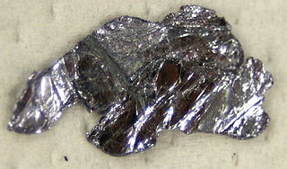
Molybdenum disulfide is an inorganic compound composed of molybdenum and sulfur. Its chemical formula is MoS2.
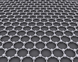
Graphene is an allotrope of carbon consisting of a single layer of atoms arranged in a honeycomb nanostructure. The name is derived from "graphite" and the suffix -ene, reflecting the fact that the graphite allotrope of carbon contains numerous double bonds in a two dimensional sheet.

Photodetectors, also called photosensors, are sensors of light or other electromagnetic radiation. There are a wide variety of photodetectors which may be classified by mechanism of detection, such as photoelectric or photochemical effects, or by various performance metrics, such as spectral response. Semiconductor-based photodetectors typically use a p–n junction that converts photons into charge. The absorbed photons make electron–hole pairs in the depletion region. Photodiodes and photo transistors are a few examples of photo detectors. Solar cells convert some of the light energy absorbed into electrical energy.
Phaedon Avouris is a Greek chemical physicist and materials scientist. He is an IBM Fellow and was formerly the group leader for Nanometer Scale Science and Technology at the Thomas J. Watson Research Center in Yorktown Heights, New York.
Saturable absorption is a property of materials where the absorption of light decreases with increasing light intensity. Most materials show some saturable absorption, but often only at very high optical intensities. At sufficiently high incident light intensity, the ground state of a saturable absorber material is excited into an upper energy state at such a rate that there is insufficient time for it to decay back to the ground state before the ground state becomes depleted, causing the absorption to saturate. The key parameters for a saturable absorber are its wavelength range, its dynamic response, and its saturation intensity and fluence.
Alex K. Zettl is an American experimental physicist, educator, and inventor.

Transparent conducting films (TCFs) are thin films of optically transparent and electrically conductive material. They are an important component in a number of electronic devices including liquid-crystal displays, OLEDs, touchscreens and photovoltaics. While indium tin oxide (ITO) is the most widely used, alternatives include wider-spectrum transparent conductive oxides (TCOs), conductive polymers, metal grids and random metallic networks, carbon nanotubes (CNT), graphene, nanowire meshes and ultra thin metal films.
A plasmonic metamaterial is a metamaterial that uses surface plasmons to achieve optical properties not seen in nature. Plasmons are produced from the interaction of light with metal-dielectric materials. Under specific conditions, the incident light couples with the surface plasmons to create self-sustaining, propagating electromagnetic waves known as surface plasmon polaritons (SPPs). Once launched, the SPPs ripple along the metal-dielectric interface. Compared with the incident light, the SPPs can be much shorter in wavelength.
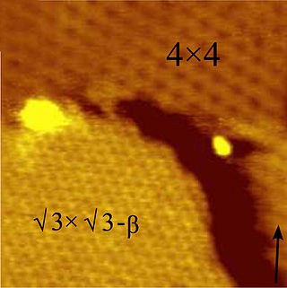
Silicene is a two-dimensional allotrope of silicon, with a hexagonal honeycomb structure similar to that of graphene. Contrary to graphene, silicene is not flat, but has a periodically buckled topology; the coupling between layers in silicene is much stronger than in multilayered graphene; and the oxidized form of silicene, 2D silica, has a very different chemical structure from graphene oxide.
Bilayer graphene is a material consisting of two layers of graphene. One of the first reports of bilayer graphene was in the seminal 2004 Science paper by Geim and colleagues, in which they described devices "which contained just one, two, or three atomic layers"
Molybdenum diselenide is an inorganic compound of molybdenum and selenium. Its structure is similar to that of MoS
2. Compounds of this category are known as transition metal dichalcogenides, abbreviated TMDCs. These compounds, as the name suggests, are made up of a transition metals and elements of group 16 on the periodic table of the elements. Compared to MoS
2, MoSe
2 exhibits higher electrical conductivity.
Valleytronics is an experimental area in semiconductors that exploits local extrema ("valleys") in the electronic band structure. Certain semiconductors have multiple "valleys" in the electronic band structure of the first Brillouin zone, and are known as multivalley semiconductors. Valleytronics is the technology of control over the valley degree of freedom, a local maximum/minimum on the valence/conduction band, of such multivalley semiconductors.
Potential graphene applications include lightweight, thin, and flexible electric/photonics circuits, solar cells, and various medical, chemical and industrial processes enhanced or enabled by the use of new graphene materials, and favoured by massive cost decreases in graphene production.

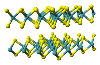
Transition-metal dichalcogenide (TMD or TMDC) monolayers are atomically thin semiconductors of the type MX2, with M a transition-metal atom (Mo, W, etc.) and X a chalcogen atom (S, Se, or Te). One layer of M atoms is sandwiched between two layers of X atoms. They are part of the large family of so-called 2D materials, named so to emphasize their extraordinary thinness. For example, a MoS2 monolayer is only 6.5 Å thick. The key feature of these materials is the interaction of large atoms in the 2D structure as compared with first-row transition-metal dichalcogenides, e.g., WTe2 exhibits anomalous giant magnetoresistance and superconductivity.
A two-dimensional semiconductor is a type of natural semiconductor with thicknesses on the atomic scale. Geim and Novoselov et al. initiated the field in 2004 when they reported a new semiconducting material graphene, a flat monolayer of carbon atoms arranged in a 2D honeycomb lattice. A 2D monolayer semiconductor is significant because it exhibits stronger piezoelectric coupling than traditionally employed bulk forms. This coupling could enable applications. One research focus is on designing nanoelectronic components by the use of graphene as electrical conductor, hexagonal boron nitride as electrical insulator, and a transition metal dichalcogenide as semiconductor.
Graphene is a 2D nanosheet with atomic thin thickness in terms of 0.34 nm. Due to the ultrathin thickness, graphene showed many properties that are quite different from their bulk graphite counterparts. The most prominent advantages are known to be their high electron mobility and high mechanical strengths. Thus, it exhibits potential for applications in optics and electronics especially for the development of wearable devices as flexible substrates. More importantly, the optical absorption rate of graphene is 2.3% in the visible and near-infrared region. This broadband absorption characteristic also attracted great attention of the research community to exploit the graphene-based photodetectors/modulators.
Graphene is a semimetal whose conduction and valence bands meet at the Dirac points, which are six locations in momentum space, the vertices of its hexagonal Brillouin zone, divided into two non-equivalent sets of three points. The two sets are labeled K and K′. The sets give graphene a valley degeneracy of gv = 2. By contrast, for traditional semiconductors the primary point of interest is generally Γ, where momentum is zero. Four electronic properties separate it from other condensed matter systems.

Twistronics is the study of how the angle between layers of two-dimensional materials can change their electrical properties. Materials such as bilayer graphene have been shown to have vastly different electronic behavior, ranging from non-conductive to superconductive, that depends sensitively on the angle between the layers. The term was first introduced by the research group of Efthimios Kaxiras at Harvard University in their theoretical treatment of graphene superlattices.
Pablo Jarillo-Herrero is a Spanish physicist and current Cecil and Ida Green Professor of Physics at Massachusetts Institute of Technology (MIT).

 A representation of graphene's band gap before and after doping (Figure 1a)
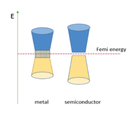 A representation of convention metal and semiconductor band gaps (Figure 1b)