PA-8000

Last updated

A HP PA-8000 microprocessor HP-HP9000-PARISC-PA8000-CPU 001 (cropped).jpg
A HP PA-8000 microprocessor

The PA-8000 (PCX-U), code-named Onyx, is a microprocessor developed and fabricated by Hewlett-Packard (HP) that implemented the PA-RISC 2.0 instruction set architecture (ISA). [1] It was a completely new design with no circuitry derived from previous PA-RISC microprocessors. The PA-8000 was introduced on 2 November 1995 when shipments began to members of the Precision RISC Organization (PRO). [2] It was used exclusively by PRO members and was not sold on the merchant market. All follow-on PA-8x00 processors (PA-8200 to PA-8900, described further below) are based on the basic PA-8000 processor core.

Contents

The PA-8000 was used by:

Description

The PA-8000 is a four-way superscalar microprocessor that executes instructions out-of-order and speculatively. [1] [3] These features were not found in previous PA-RISC implementations, making the PA-8000 the first PA-RISC CPU to break the tradition of using simple microarchitectures and high-clock rate implementation to attain performance. [4]

Instruction fetch unit

The PA-8000 has a four-stage front-end. During the first two stages, four instructions are fetched from the instruction cache by the instruction fetch unit (IFU). [4] The IFU contains the program counter, branch history table (BHT), branch target address cache (BTAC) and a four-entry translation lookaside buffer (TLB). [1] [4] The TLB is used to translate virtual address to physical addresses for accessing the instruction cache. In the event of a TLB miss, the translation is requested from the main TLB. [1]

Branch prediction

The PA-8000 performs branch prediction using static or dynamic methods. [1] Which method the PA-8000 used was selected by a bit in each TLB entry. Static prediction considers most backwards branches as taken and forward branches as not taken. Static prediction also predicted the outcome of branches by examining hints encoded in the instructions themselves by the compiler. [1] [4]

Dynamic prediction uses the recorded history of a branch to decide whether it is taken or not taken. A 256-entry BHT is where this information is stored. Each BHT entry is a three-bit shift register. The PA-8000 used a majority vote algorithm, a branch is taken if the majority of the three bits are set, and not taken if they are clear. [1] A mispredicted branch causes a five-cycle penalty. [4] The BHT is updated when the outcome of the branch is known. Although the PA-8000 can execute two branch instructions per cycle, only one of the outcomes is recorded as the BHT is not dual-ported to simplify its implementation. [3]

The PA-8000 has a two-cycle bubble for correctly predicted branches, as the target address of the branch must be calculated before it is sent to the instruction cache. [4] To reduce the occurrence of this bubble, the PA-8000 uses a 32-entry fully associative BTAC. The BTAC caches a branch's target address. When the same branch is encountered, and is predicted as taken, the address is sent to the instruction cache immediately, allowing the fetch to begin without delay. [1]

To maximize the effectiveness of the BTAC, only the branch target of predicted-taken branches are cached. If a branch is predicted as not taken, but its target address is cached in the BTAC, its entry is deleted. In the event that the BTAC is full, and a new entry needs to be written, the entry that is replaced is selected using a round robin replacement policy. [1]

Instruction cache

The instruction cache is external and supports a capacity of 256 KB to 4 MB. Instructions are pre-decoded before they enter the cache by adding five bits to each instruction. These bits reduce the amount of time required to decode the instruction later in the pipeline. The instruction cache is direct-mapped to avoid the complexity of set associative caches and is accessed via a 148-bit bus. The tags for the cache are also external. It is built from synchronous SRAMs (SSRAMs).

Decode, and the instruction reorder buffer

During the third stage, the instructions are decoded. In the fourth stage, they are placed in the instruction reorder buffer (IRB). The IRB's purpose is the implement register renaming, out of order execution, speculative execution and to provide a temporary place for results to be stored until the instructions are retired. The IRB determines which instructions are issued during stage five.

The IRB consists of two buffers, one for integer and floating-point instructions, the other for load and store instructions. Some instructions are placed into both buffers. These instructions are branch instructions and certain system instructions. Each buffer has 28 entries. Each buffer can accept up to four instructions per cycle and can issue up to two per a cycle to its functional units.

Execution

All instructions begin execution during stage six in the ten functional units. Integer instructions except for multiply are executed in two arithmetic logic units (ALUs) and two shift/merge units. All instructions executed in these units have a single-cycle latency and their results are written to the destination register in stage seven.

Floating-point instructions and integer multiply instructions are executed in two fused multiply–accumulate (FMAC) units and two divide/square-root units. The FMAC units are pipelined and have a three-cycle latency. Multiplication is performed during stage six, addition in stage seven, rounding in stage eight and writeback in stage nine. There is no rounding between the multiply and accumulate stages. The FMAC units also execute individual multiply and add instructions, which also have a latency of three cycles for both single-precision and double-precision variants. The divide/square-root units are not pipelined and have a 17-cycle latency. One instruction can be issued to them per clock cycle due to register port limitations, but they can operate in parallel with each other and the FMAC units.

Both integer and floating-point load and store instructions are executed by two dedicated address adders.

Translation lookaside buffer

The translation lookaside buffer (TLB) contains 96 entries and is dual-ported and full-associative. It can translate two virtual addresses per cycle. This TLB translates addresses for both instructions and data. When the IFU's TLB misses, this TLB provides the translation for it. Translation for loads and stores have a higher priority than those for instructions. Each TLB entry can be mapped to a page with a size between 4 KB to 16 MB, in increments that are powers of four.

Data cache

The PA-8000 has a data cache with a capacity up to 4 MB. The data cache is dual-ported, so two reads or writes can be performed during every cycle. It is dual-ported by implementing two banks of cache, thus it is not truly dual-ported because if two reads or writes reference the same bank, a conflict arises and only one operation can be performed. It is accessed by two 64-bit buses, one for each bank. The cache tags are external. There are two copies of the cache tags to allow independent accesses in each bank. The data cache is direct-mapped for the same reasons as the instruction cache. It is built from SSRAMs.

Runway bus

The external interface is the Runway bus, a 64-bit address and data multiplexed bus. The PA-8000 uses a 40-bit physical address, thus it is able to address 1 TB of physical memory.

Physical

A HP PA-8000 microprocessor (top and bottom view) HP-HP9000-PARISC-PA8000-CPU 010 (cropped).jpg
A HP PA-8000 microprocessor (top and bottom view)

The PA-8000 has 3.8 million transistors and measures 17.68 mm by 19.10 mm, [5] for an area of 337.69 mm2. It was fabricated by HP in their CMOS-14C process, a 10% gate shrink of the CMOS-14 process. [4] The CMOS-14C process was a 0.5 μm, five-level aluminum interconnect, complementary metal–oxide–semiconductor (CMOS) process. The die has 704 solder bumps for signals and 1,200 for power or ground. It is packaged in a 1,085-pad flip chip alumina ceramic land grid array (LGA). [6] The PA-8000 uses a 3.3 V power supply.

PA-8200

A HP PA-8200 microprocessor HP-HP9000-PARISC-PA8200-CPU 001 (cropped).jpg
A HP PA-8200 microprocessor

The PA-8200 (PCX-U+), code-named Vulcan, was a further development of the PA-8000. The first systems to use the PA-8200 became available in June 1997. The PA-8200 operated at 200 to 240 MHz and primarily competed with the Alpha 21164. Improvements were made to branch prediction and the TLB. [3] [7] Branch prediction was improved by quadrupling the number of BHT entries to 1,024, which required the use of a two-bit algorithm in order to fit without redesign of surrounding circuitry; and by implementing a write queue that enabled two branch outcomes to be recorded by the BHT instead of one. The number of TLB entries was increased to 120 entries from 96, which reduced TLB misses. The clock frequency was also improved through minor circuit redesign. The PA-8200's die was identical in size to the PA-8000 as improvements utilized empty areas of the die. It was fabricated in the CMOS-14C process.

PA-8500

A HP PA-8500 microprocessor (top and bottom view) HP-HP9000-PARISC-PA8500-CPU 001 (cropped).jpg
A HP PA-8500 microprocessor (top and bottom view)

The PA-8500 (PCX-W), code-named Barracuda, is a further development of the PA-8200. It taped-out in early 1998 and was introduced in late-1998 within systems. Production versions operated at frequencies of 300 to 440 MHz, but it was designed to, and has, operated up to 500 MHz. [8] The most notable improvements are the higher operating frequencies and the on-die integration of the primary caches. [9] The higher operating frequencies and the integration of the primary caches on the same die as the core was enabled by the migration to a 0.25 μm process. The PA-8500 core measured 10.8 mm by 11.4 mm (123.12 mm2) in the new process, less than half the area of the 0.5 μm PA-8200. This made area available that could be used for integrating the caches.

The PA-8500 has a 512 KB instruction cache and a 1 MB data cache. Other improvements to the microarchitecture include a larger BHT containing 2,048 entries, twice the capacity of the PA-8200's, and a larger TLB containing 160 entries. The PA-8500 uses a new version of the Runway bus. The new version operates at 125 MHz and transfers data on both rising and falling edges of the clock signal (double data rate, or DDR) and yields 240 MT/s or 2 GB/s of bandwidth. As the Runway bus is used to transfer addresses and data, usable bandwidth is 80% that of 2 GB/s, or around 1.6 GB/s.

The PA-8500 contains 140 million transistors and measures 21.3 mm by 22.0 mm (468.6 mm2). [8] It was fabricated by Intel Corporation in a 0.25 μm CMOS process with five levels of aluminium interconnect. It uses a 2.0 V power supply. HP did not fabricate the PA-8500 themselves as they had ceased to upgrade their fabs to implement a process newer than CMOS-14C, which was used to fabricate previous PA-RISC microprocessors.

The PA-8500 was packaged in a smaller 544-pad land grid array (LGA) as the integration of the primary caches on die resulted in the removal of the two 128-bit buses which communicated with the external caches and their associated I/O pads.

PA-8600

A HP PA-8600 microprocessor HP-HP9000-PARISC-PA8600-CPU 001 (cropped).jpg
A HP PA-8600 microprocessor

The PA-8600 (PCX-W+), code-named Landshark, is a further development of the PA-8500 introduced in January 2000. The PA-8600 was intended to be introduced in mid-2000. [10] It was a tweaked version of the PA-8500 to enable it to reach higher clock frequencies of 480 to 550 MHz. It improved the microarchitecture by using a quasi-least recently used (LRU) eviction policy for instruction cache. It was fabricated by Intel.

PA-8700

A HP PA-8700 microprocessor HP-HP9000-PARISC-PA8700-CPU 002 (cropped).jpg
A HP PA-8700 microprocessor

The PA-8700 (PCX-W2), code-named Piranha, is a further development of the PA-8600. Introduced in August 2001, it operated at 625 to 750 MHz. Improvements were the implementation of data prefetching, a quasi-LRU replacement policy for the data cache, and a larger 44-bit physical address space to address 16 TB of physical memory. [11] The PA-8700 also has larger instruction and data caches, increased in capacity by 50% to 0.75 MB and 1.5 MB, respectively. The PA-8700 was fabricated by IBM Microelectronics [12] in a 0.18 μm silicon on insulator (SOI) CMOS process with seven levels of copper interconnect and low-κ dielectric.

PA-8700+

The PA-8700+ was a further development of the PA-8700 introduced in systems in mid-2002. It operated at 875 MHz. [12]

PA-8800

A HP PA-8800 microprocessor HP-HP9000-PARISC-PA8800-CPU 001 (cropped).jpg
A HP PA-8800 microprocessor
PA-8000 CPU module with the four ESRAMs HP-HP9000-PARISC-PA8800-CPU 004.jpg
PA-8000 CPU module with the four ESRAMs

The PA-8800, code-named Mako, is a further development of the PA-8700. [13] It was introduced in 2004 and was used by HP in their C8000 workstation and HP 9000 Superdome servers. It was available at 0.8, 0.9 and 1.0 GHz. The PA-8800 was a dual-core design consisting of two modified PA-8700+ microprocessors on a single die. Each core has a 768 KB instruction cache and a 768 KB data cache. The primary caches are smaller than those in the PA-8700 to enable both cores to fit on the same die.

Improvements over the PA-8700 are improved branch prediction and the inclusion of an external 32 MB unified secondary cache. The secondary cache has a bandwidth of 10 GB/s and a latency of 40 cycles. It is 4-way set-associative, physically indexed and physically tagged with a line size of 128 bytes. The set-associativity was chosen to reduce the number of I/O pins. The L2 cache is implemented with using four 72 Mbit (9 MB) Enhanced Memory Systems Enhanced SRAM (ESRAM) chips, which despite its name, is an implementation of 1T-SRAM dynamic random access memory (DRAM) with a SRAM-like interface. Access to this cache by each core is arbitrated by the on-die controller and the 1 MB of secondary cache tags also resides on-die as SRAM and is protected by ECC. The PA-8800 used the same front side bus as the McKinley Itanium microprocessor, which yields 6.4 GB/s of bandwidth, and is compatible with HP's Itanium chipsets such as the zx1.

It consisted of 300 million transistors, of which 25 million were for logic, on a 23.6 mm by 15.5 mm (365.8 mm2) die. [13] It was fabricated by IBM in 0.13 μm SOI process with copper interconnects and low-κ dielectric. The PA-8800 is packaged in a ceramic ball grid array mounted on a printed circuit board (PCB) with the four ESRAMs, forming a module similar to those used by early Itanium microprocessors.

PA-8900

A HP PA-8900 microprocessor HP-HP9000-PARISC-PA8900-CPU 001 (cropped).jpg
A HP PA-8900 microprocessor
PA-8000 CPU module with the four ESRAMs HP-HP9000-PARISC-PA8900-CPU 002.jpg
PA-8000 CPU module with the four ESRAMs

The PA-8900, code-named Shortfin, was a derivative of the PA-8800. It was the last PA-RISC microprocessor to be developed and was introduced on 31 May 2005 when systems using the microprocessor became available. It was used in the HP 9000 servers and the C8000 workstation. It operated at 0.8, 0.9, 1.0 and 1.1 GHz. It is not a die shrink of the PA-8800, as was earlier rumored. The L2 cache was doubled in capacity to 64 MB, has lower latency, and better error detection and correction on caches. It uses the McKinley system bus and was compatible with Itanium 2 chipsets such as the HP zx1. There were no microarchitecture changes, but the floating-point unit and on-die cache circuitry was redesigned to reduce power consumption, and each core subsequently dissipated approximately 35 W at 1.0 GHz.

Notes

  1. 1 2 3 4 5 6 7 8 9 Hunt 1995
  2. "HP Announces Release of PA-8000 to PRO Partners".
  3. 1 2 3 Scott 1997
  4. 1 2 3 4 5 6 7 Gwennap 1994
  5. Gaddis 1996, p. 1697
  6. Kumar, "The HP PA-8000 RISC CPU"
  7. Gwennap 1996
  8. 1 2 Barnes 1999
  9. Gwennap 1997
  10. Wermer, "HP's PA-8600 processor earlier to ship than expected".
  11. Krewell 2000
  12. 1 2 ComputerWire 2002
  13. 1 2 Johnson 2001, p. 1

Related Research Articles

<span class="mw-page-title-main">PA-RISC</span> Instruction set architecture by Hewlett-Packard

Precision Architecture RISC (PA-RISC) or Hewlett Packard Precision Architecture, is a general purpose computer instruction set architecture (ISA) developed by Hewlett-Packard from the 1980s until the 2000s.

<span class="mw-page-title-main">UltraSPARC</span> Microprocessor developed by Sun Microsystems

The UltraSPARC is a microprocessor developed by Sun Microsystems and fabricated by Texas Instruments, introduced in mid-1995. It is the first microprocessor from Sun to implement the 64-bit SPARC V9 instruction set architecture (ISA). Marc Tremblay was a co-microarchitect.

<span class="mw-page-title-main">HP 9000</span> Line of workstation and server computer systems

HP 9000 is a line of workstation and server computer systems produced by the Hewlett-Packard (HP) Company. The native operating system for almost all HP 9000 systems is HP-UX, which is based on UNIX System V.

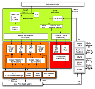
The Runway bus is a front-side bus developed by Hewlett-Packard for use by its PA-RISC microprocessor family. The Runway bus is a 64-bit wide, split transaction, time multiplexed address and data bus running at 120 MHz. This scheme was chosen by HP as they determined that a bus using separate address and data wires would have only delivered 20% more bandwidth for a 50% increase in pin count, which would have made microprocessors using the bus more expensive. The Runway bus was introduced with the release of the PA-7200 and was subsequently used by the PA-8000, PA-8200, PA-8500, PA-8600 and PA-8700 microprocessors. Early implementations of the bus used in the PA-7200, PA-8000 and PA-8200 had a theoretical bandwidth of 960 MB/s. Beginning with the PA-8500, the Runway bus was revised to transmit on both rising and falling edges of a 125 MHz clock signal, which increased its theoretical bandwidth to 2 GB/s. The Runway bus was succeeded with the introduction of the PA-8800, which used the Itanium 2 bus.

SPARC64 is a microprocessor developed by HAL Computer Systems and fabricated by Fujitsu. It implements the SPARC V9 instruction set architecture (ISA), the first microprocessor to do so. SPARC64 was HAL's first microprocessor and was the first in the SPARC64 brand. It operates at 101 and 118 MHz. The SPARC64 was used exclusively by Fujitsu in their systems; the first systems, the Fujitsu HALstation Model 330 and Model 350 workstations, were formally announced in September 1995 and were introduced in October 1995, two years late. It was succeeded by the SPARC64 II in 1996.

<span class="mw-page-title-main">AMD Am29000</span> Family of RISC microprocessors and microcontrollers

The AMD Am29000, commonly shortened to 29k, is a family of 32-bit RISC microprocessors and microcontrollers developed and fabricated by Advanced Micro Devices (AMD). Based on the seminal Berkeley RISC, the 29k added a number of significant improvements. They were, for a time, the most popular RISC chips on the market, widely used in laser printers from a variety of manufacturers.

<span class="mw-page-title-main">R10000</span> MIPS microprocessor

The R10000, code-named "T5", is a RISC microprocessor implementation of the MIPS IV instruction set architecture (ISA) developed by MIPS Technologies, Inc. (MTI), then a division of Silicon Graphics, Inc. (SGI). The chief designers are Chris Rowen and Kenneth C. Yeager. The R10000 microarchitecture is known as ANDES, an abbreviation for Architecture with Non-sequential Dynamic Execution Scheduling. The R10000 largely replaces the R8000 in the high-end and the R4400 elsewhere. MTI was a fabless semiconductor company; the R10000 was fabricated by NEC and Toshiba. Previous fabricators of MIPS microprocessors such as Integrated Device Technology (IDT) and three others did not fabricate the R10000 as it was more expensive to do so than the R4000 and R4400.

<span class="mw-page-title-main">R4000</span> MIPS microprocessor

The R4000 is a microprocessor developed by MIPS Computer Systems that implements the MIPS III instruction set architecture (ISA). Officially announced on 1 October 1991, it was one of the first 64-bit microprocessors and the first MIPS III implementation. In the early 1990s, when RISC microprocessors were expected to replace CISC microprocessors such as the Intel i486, the R4000 was selected to be the microprocessor of the Advanced Computing Environment (ACE), an industry standard that intended to define a common RISC platform. ACE ultimately failed for a number of reasons, but the R4000 found success in the workstation and server markets.

The R8000 is a microprocessor chipset developed by MIPS Technologies, Inc. (MTI), Toshiba, and Weitek. It was the first implementation of the MIPS IV instruction set architecture. The R8000 is also known as the TFP, for Tremendous Floating-Point, its name during development.

<span class="mw-page-title-main">POWER2</span> 1993 family of microprocessors by IBM

The POWER2, originally named RIOS2, is a processor designed by IBM that implemented the POWER instruction set architecture. The POWER2 was the successor of the POWER1, debuting in September 1993 within IBM's RS/6000 systems. When introduced, the POWER2 was the fastest microprocessor, surpassing the Alpha 21064. When the Alpha 21064A was introduced in 1993, the POWER2 lost the lead and became second. IBM claimed that the performance for a 62.5 MHz POWER2 was 73.3 SPECint92 and 134.6 SPECfp92.

<span class="mw-page-title-main">VAX 8000</span> Family of superminicomputers by Digital Equipment Corporation

The VAX 8000 is a discontinued family of superminicomputers developed and manufactured by Digital Equipment Corporation (DEC) using processors implementing the VAX instruction set architecture (ISA).

<span class="mw-page-title-main">Alpha 21064</span> Microprocessor

The Alpha 21064 is a microprocessor developed and fabricated by Digital Equipment Corporation that implemented the Alpha instruction set architecture (ISA). It was introduced as the DECchip 21064 before it was renamed in 1994. The 21064 is also known by its code name, EV4. It was announced in February 1992 with volume availability in September 1992. The 21064 was the first commercial implementation of the Alpha ISA, and the first microprocessor from Digital to be available commercially. It was succeeded by a derivative, the Alpha 21064A in October 1993. This last version was replaced by the Alpha 21164 in 1995.

<span class="mw-page-title-main">Alpha 21164</span> Microprocessor

The Alpha 21164, also known by its code name, EV5, is a microprocessor developed and fabricated by Digital Equipment Corporation that implemented the Alpha instruction set architecture (ISA). It was introduced in January 1995, succeeding the Alpha 21064A as Digital's flagship microprocessor. It was succeeded by the Alpha 21264 in 1998.

<span class="mw-page-title-main">Alpha 21264</span> RISC microprocessor

The Alpha 21264 is a Digital Equipment Corporation RISC microprocessor launched on 19 October 1998. The 21264 implemented the Alpha instruction set architecture (ISA).

The SPARC64 V (Zeus) is a SPARC V9 microprocessor designed by Fujitsu. The SPARC64 V was the basis for a series of successive processors designed for servers, and later, supercomputers.

The R2000 is a 32-bit microprocessor chip set developed by MIPS Computer Systems that implemented the MIPS I instruction set architecture (ISA). Introduced in January 1986, it was the first commercial implementation of the MIPS architecture and the first commercial RISC processor available to all companies. The R2000 competed with Digital Equipment Corporation (DEC) VAX minicomputers and with Motorola 68000 and Intel Corporation 80386 microprocessors. R2000 users included Ardent Computer, DEC, Silicon Graphics, Northern Telecom and MIPS's own Unix workstations.

The R4200 is a microprocessor designed by MIPS Technologies, Inc. (MTI) that implemented the MIPS III instruction set architecture (ISA). It was also known as the VRX during development. The microprocessor was licensed to NEC, and the company fabricated and marketed it as the VR4200. The first VR4200, an 80 MHz part, was introduced in 1993. A faster 100 MHz part became available in 1994.

The PA-7200 – also known as PCX-T', code-named Thunderbird' –, is a microprocessor that implements the PA-RISC 1.1 instruction set architecture (ISA) developed by Hewlett-Packard (HP). It was introduced in early 1995, debuting in systems from HP. The PA-7200 was not sold openly and the only third-party users were Convex Computer and Stratus Computer, both members of the Precision RISC Organization (PRO). It was developed for small multiprocessing systems with two or four microprocessors. The microprocessor was first described at the Compcon and IEEE International Solid-State Circuits Conference (ISSCC) conferences.

<span class="mw-page-title-main">PA-7100LC</span> Microprocessor developed by Hewlett-Packard

The PA-7100LC is a microprocessor that implements the PA-RISC 1.1 instruction set architecture (ISA) developed by Hewlett-Packard (HP). It is also known as the PCX-L, and by its code-name, Hummingbird. It was designed as a low-cost microprocessor for low-end systems. The first systems to feature the PA-7100LC were introduced in January 1994. These systems used 60 and 80 MHz clock rates. A 100 MHz part debuted in June 1994. The PA-7100LC was the first PA-RISC microprocessor to implement the MAX-1 multimedia instructions, an early single instruction, multiple data (SIMD) multimedia instruction set extension that provided instructions for improving the performance of MPEG video decoding.

<span class="mw-page-title-main">R4600</span>

The R4600, code-named "Orion", is a microprocessor developed by Quantum Effect Design (QED) that implemented the MIPS III instruction set architecture (ISA). As QED was a design firm that did not fabricate or sell their designs, the R4600 was first licensed to Integrated Device Technology (IDT), and later to Toshiba and then NKK. These companies fabricated the microprocessor and marketed it. The R4600 was designed as a low-end workstation or high-end embedded microprocessor. Users included Silicon Graphics, Inc. (SGI) for their Indy workstation and DeskStation Technology for their Windows NT workstations. The R4600 was instrumental in making the Indy successful by providing good integer performance at a competitive price. In embedded systems, prominent users included Cisco Systems in their network routers and Canon in their printers.

References

Further reading